🔍 Executive Summary
- Samsung Foundry is witnessing a recovery in its 4nm production line utilization, driven by a surge in AI chip projects and the strategic integration of HBM4 technology into its advanced process ecosystem.
Strategic Deep-Dive
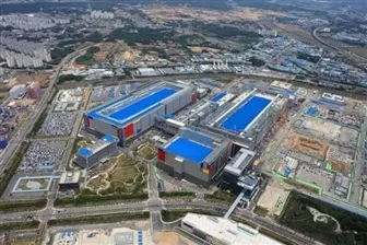
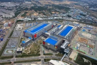
Samsung Electronics’ foundry division is orchestrating a formidable comeback, capitalizing on the insatiable global demand for AI-centric silicon. After a challenging period marked by yield concerns and underutilized capacity, the company is now seeing its 4nm production lines reach high utilization rates. This revitalization is not a product of chance; it is a calculated result of Samsung’s alignment with the AI accelerator market and the upcoming HBM4 transition.
As a Lead Data Architect would observe, we are witnessing the consolidation of the ‘Logic-Memory’ wall, where Samsung’s unique position as an Integrated Device Manufacturer (IDM) provides a distinct competitive edge.
The 4nm node has emerged as the industry’s workhorse for high-performance AI hardware. It offers a mature and cost-effective alternative to the ultra-premium 3nm nodes, providing the necessary Power-Performance-Area (PPA) metrics for Large Language Model (LLM) inference engines and edge AI processors. Samsung’s ability to stabilize yields at this node has allowed it to recapture market share from fabless clients who previously migrated to competitors.
The technical refinement of the 4nm process—specifically improved gate-oxide quality and interconnect reliability—has reduced the leakage current, a critical factor for AI chips that operate under high thermal stress.
However, the true catalyst for this foundry rebound is the strategic integration of HBM4. Unlike previous generations, HBM4 moves the memory interface closer to the logic die, requiring sophisticated Through-Silicon Via (TSV) technology and hybrid bonding techniques. Samsung’s ‘One-Stop’ service model—where it fabricates the logic die on its 4nm or 3nm lines and then bundles it with its proprietary HBM4 stacks—is a powerful value proposition.
This vertical integration reduces the I/O density bottlenecks and interconnect latencies that often plague decoupled supply chains. For hyperscalers designing custom silicon, this eliminates the complexity of coordinating between separate memory vendors and foundries, significantly accelerating time-to-market.
Moreover, the surge in 4nm demand serves as a vital bridge to Samsung’s 3nm and 2nm Gate-All-Around (GAA) roadmap. The data gathered from high-volume 4nm production is being fed into the machine learning models that optimize its next-generation lithography steps. As AI startups and established tech giants seek more diverse foundry options to mitigate supply risks, Samsung’s improved operational metrics are making it an attractive alternative to TSMC.
The foundry’s recovery is more than just a financial rebound; it is a repositioning of Samsung as a vital architect of the AI hardware era, capable of delivering the holistic systems-on-chip that will power the next decade of computational intelligence.