🔍 Executive Summary
- The semiconductor materials market reached a historic milestone of US$73.2 billion in 2025, driven by a 6.8% growth rate as manufacturers scale operations to meet high-performance computing demands.
Strategic Deep-Dive
The global semiconductor materials market has surpassed all previous benchmarks, reaching a staggering US$73.2 billion in total revenue for the year 2025. According to the Materials Market Data Subscription (MMDS) report published by SEMI on May 13, 2026, this 6.8% year-over-year increase signals a robust expansion phase in the semiconductor value chain. From the vantage point of a Lead Data Architect and industry analyst, this growth trajectory is a direct consequence of the increasing material intensity required by modern silicon architectures, specifically those tailored for Artificial Intelligence and high-performance computing (HPC).
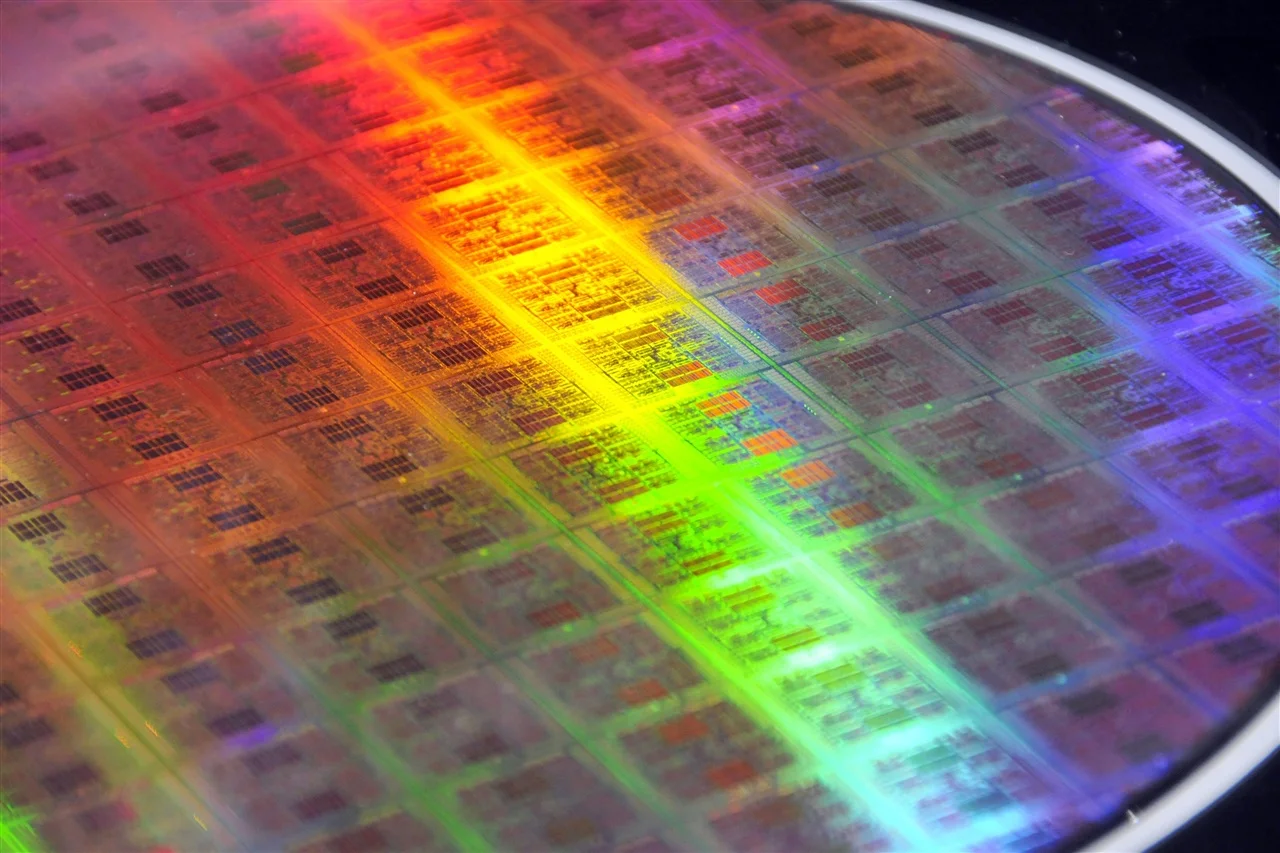
To understand the mechanics of this record-breaking figure, one must dissect the sub-segments of the market. Wafer fabrication materials, which constitute the lion’s share of this revenue, have seen heightened demand for high-purity wet chemicals, specialized gases, and advanced photoresists. As the industry migrates toward sub-3nm nodes, the consumption of Extreme Ultraviolet (EUV) photoresists has escalated, given the multiple patterning steps required to maintain precision at the atomic scale.
Furthermore, the volume of Chemical Mechanical Planarization (CMP) slurries used per wafer has increased as designs move toward complex, multi-layered 3D structures. These materials are not just commodities; they are the enabling agents for yield optimization in high-stakes fabrication environments.
The packaging materials sector has also undergone a transformative shift. The rise of heterogeneous integration and chiplet architectures has necessitated a new class of materials. Advanced substrates, specifically Ajinomoto Build-up Film (ABF) and high-density interconnects, have faced supply constraints as demand for AI accelerators surged.
The integration of High Bandwidth Memory (HBM) requires specialized thermal interface materials (TIM) and underfills to manage the high heat flux generated by stacked dies. This ’thermal envelope’ management is a critical architectural concern, making high-performance packaging materials a high-margin growth engine for the industry.
Geographically, the revenue concentration mirrors the global manufacturing footprint. Taiwan remains the dominant consumer of semiconductor materials, followed closely by South Korea and Mainland China. These regions have aggressively expanded their wafer start capacities to alleviate the global chip shortage of previous years, leading to a consistent pull on the materials supply chain.
The 6.8% growth rate also reflects a pricing premium for ‘green’ and sustainable chemicals, as ESG mandates force manufacturers to seek alternatives to traditional hazardous precursors. Looking ahead, the Materials Market Data Subscription suggests that the market will continue to expand as the industry prepares for the transition to 2nm nodes and the mass adoption of HBM4, where the complexity of material synthesis will once again redefine the ceiling for semiconductor performance and profitability.