🔍 Executive Summary
- The AI-driven demand for high-performance memory has triggered a massive CapEx race between Samsung and SK Hynix, as both giants rush to expand HBM and DRAM fabrication capacities to secure dominance in the next-generation hardware stack.
Strategic Deep-Dive
The semiconductor industry is witnessing a tectonic shift driven by the unrelenting artificial intelligence boom, which has triggered an unprecedented expansion race between Samsung Electronics and SK Hynix. This is not a typical cyclical capacity increase; it is a structural surge in Capital Expenditure (CapEx) aimed at eliminating the memory wall—the primary bottleneck in modern AI compute. As AI workloads migrate toward increasingly complex Large Language Models (LLMs), the demand for High Bandwidth Memory (HBM) and high-density DDR5 modules has outpaced all previous industry forecasts, forcing these giants into a race for technological and physical supremacy.
From a Systems Architect’s perspective, the HBM race is a battle of packaging and interconnect density. SK Hynix, currently holding a significant lead in the HBM3e market, is doubling down on its proprietary Mass Reflow-Molded Underfill (MR-MUF) technology, which offers superior thermal management and structural integrity for high-stack architectures. Meanwhile, Samsung Electronics is leveraging its massive financial reserves and integrated device manufacturing (IDM) capabilities to scale up High-NA EUV-based DRAM production.
Samsung’s focus is on the next-generation HBM4 standard, where the integration of the memory stack directly onto logic dies using advanced Through-Silicon Via (TSV) technology will redefine the PPA (Power, Performance, Area) metrics of AI accelerators.
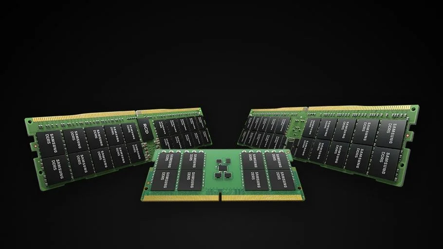
The manufacturing complexity of these devices is staggering. Producing a 12-layer or 16-layer HBM stack requires precision and yield rates that push the boundaries of materials science. The “packaging bottleneck” has become the new industry reality, prompting both companies to build dedicated advanced packaging facilities.
SK Hynix’s investment in global production sites and Samsung’s focus on a comprehensive “one-stop shop” for logic, memory, and packaging indicate a shift from commodity supply to a partnership-driven infrastructure model. Both firms are racing to secure long-term supply agreements with AI hyperscalers and GPU designers, recognizing that in the AI era, capacity equals influence.
However, this aggressive expansion is a high-stakes gamble. The industry is haunted by the specter of oversupply, a recurring theme in memory market history. If the AI growth trajectory plateaus, the massive fabs currently under construction could lead to a significant supply-demand imbalance.
Nevertheless, the risk of under-capacity is viewed as more existential. In a world where AI capabilities are constrained by memory bandwidth, being unable to meet the needs of the leading hyperscalers could result in a permanent loss of market leadership. As we approach the HBM4 era, where memory becomes semi-custom silicon, the outcome of this capacity race will determine which company dictates the architectural standards of the global AI ecosystem for the next decade.