🔍 Executive Summary
- Samsung Electronics is undergoing a critical strategic realignment, pivoting away from its HBM-centric 'catch-up mode' to revive long-term investments in 3D NAND and revolutionary glass substrate technologies.
Strategic Deep-Dive
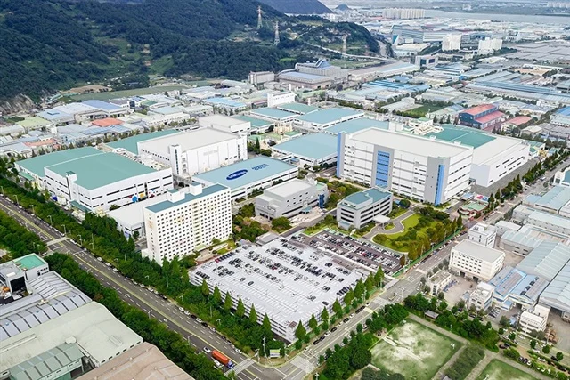
Samsung Electronics is reportedly executing a drastic and critical strategic pivot, signaling an end to its more than year-long intensive focus on High Bandwidth Memory (HBM) and DRAM design. This ’emergency’ focus was a direct response to the company falling behind competitors like SK Hynix in the AI memory gold rush, a period marked by a reactive ‘catch-up mode’ that strained its R&D resources. However, the latest internal reports indicate that Samsung is now reviving a suite of delayed semiconductor initiatives, including next-generation 3D NAND flash, compound semiconductors, and advanced substrate technologies.
This move is interpreted by industry analysts not just as an expansion, but as a strategic admission that competing solely on HBM ground is insufficient for long-term dominance.
A central pillar of this new strategy is the acceleration of glass substrate development. As the industry moves toward heterogeneous integration and 2.5D/3D packaging, traditional organic substrates are reaching their physical limits regarding thermal expansion and wiring density. Glass substrates offer superior flatness and stability, providing an ideal foundation for the massive chiplets and integrated optical engines—like TSMC’s COUPE—that will define the next decade of AI accelerators.
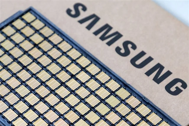
By fast-tracking glass substrate production, Samsung aims to leapfrog the current packaging paradigm and offer a superior platform for the world’s leading chip designers. Simultaneously, the company is refocusing on its traditional stronghold: 3D NAND. With the rise of AI training clusters, the demand for high-capacity, high-speed enterprise SSDs is surging, and Samsung intends to leverage its manufacturing scale to regain an unassailable lead in NAND stacking technology.
Critically, this pivot represents a return to Samsung’s core identity as a ’long-term technology trendsetter’ rather than a fast follower. For the past year, Samsung’s brand was somewhat tarnished by its perceived struggle to qualify its latest HBM3E chips for major clients, leading to a sense of strategic drift. By refocusing on the foundational elements of semiconductor manufacturing—such as advanced packaging materials and non-volatile memory—Samsung is betting that the AI market will eventually shift its bottleneck from memory speed to data storage and chip interconnectivity.
While some critics argue that this shift might be a late reaction to the HBM setback, others see it as a shrewd maneuver to dominate the ’next frontier’ where competitors are not yet firmly entrenched. The success of this pivot depends on Samsung’s ability to execute these complex technological transitions simultaneously while maintaining its foundry ambitions. This strategic realignment is a high-stakes gamble to redefine the competitive landscape, moving beyond the current HBM hype to secure the underlying infrastructure of the 2030s AI economy.
Samsung is essentially declaring that while it may have lost a battle in HBM, it plans to win the war by controlling the advanced materials and storage architectures that will eventually sustain the AI revolution.