🔍 Executive Summary
- The global buildout of hyperscale AI data centers has triggered a fundamental architectural shift in networking infrastructure, placing advanced Printed Circuit Board (PCB) technologies at the heart of the hardware revolution. As AI workloads transition from experimental models to massive distributed training environments, the efficiency of inter-server communication has become the ultimate arbiter of system performance. Standard PCB designs, which were sufficient for traditional cloud computing, are now proving inadequate for the rigors of high-speed AI networking. The industry is consequentl...
Strategic Deep-Dive
The global buildout of hyperscale AI data centers has triggered a fundamental architectural shift in networking infrastructure, placing advanced Printed Circuit Board (PCB) technologies at the heart of the hardware revolution. As AI workloads transition from experimental models to massive distributed training environments, the efficiency of inter-server communication has become the ultimate arbiter of system performance. Standard PCB designs, which were sufficient for traditional cloud computing, are now proving inadequate for the rigors of high-speed AI networking.
The industry is consequently pivoting toward sophisticated solutions capable of supporting 800G and 1.6T transmission speeds, necessitated by the massive data throughput requirements of contemporary GPU clusters. This shift represents a transition from viewing PCBs as passive structural components to recognizing them as critical high-performance interfaces designed for signal integrity and thermal management.
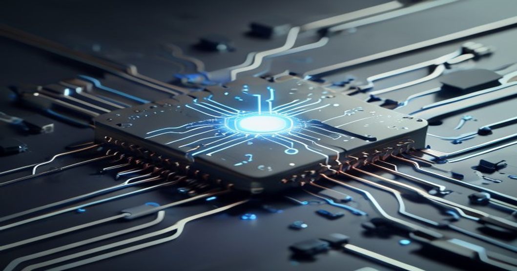
Technically, the move toward advanced PCB technologies is defined by several key innovations, most notably High-Density Interconnect (HDI) and the utilization of ultra-low-loss materials. For AI servers to function effectively, signal attenuation must be minimized at frequencies that were previously reserved for telecommunications infrastructure. This requires the use of specialized Copper Clad Laminates (CCL) with low dielectric constants (Dk) and dissipation factors (Df).
Furthermore, the sheer complexity of AI accelerators necessitates multi-layer boards (MLB) that can exceed 20 to 30 layers, requiring extreme precision in substrate thinning and interconnect density. These high-spec boards must also account for significant thermal dissipation; as power density in AI racks climbs toward 100kW and beyond, the PCB itself must act as a part of the thermal management strategy, utilizing innovative materials to prevent signal distortion caused by heat.
The economic implications of this transition are immense for the hardware supply chain. As hyperscalers like Microsoft, Google, and Meta race to deploy Blackwell-class and next-generation AI nodes, the demand for premium PCB solutions is projected to experience exponential growth. This creates a lucrative niche for manufacturers who possess the specialized technical expertise and high-precision equipment required for HDI and advanced CCL production.
The AI infrastructure boom is essentially decoupling the high-end PCB market from the broader consumer electronics cycle, establishing it as a strategic sector characterized by high margins and high barriers to entry. In essence, the ‘pipes’ through which AI data flows are being rebuilt, and the evolution of PCB technology is the primary enabler of this increased interconnect density. This trend underscores a broader reality in the tech industry: the AI revolution is as much a challenge of material science and hardware engineering as it is of software development, with the physical layer becoming the new frontier for competitive advantage.