🔍 Executive Summary
- TSMC is aggressively scaling its global manufacturing footprint with 18 new facilities to cement its dominance in the AI chip supply chain through advanced 3DFabric packaging technologies.
Strategic Deep-Dive
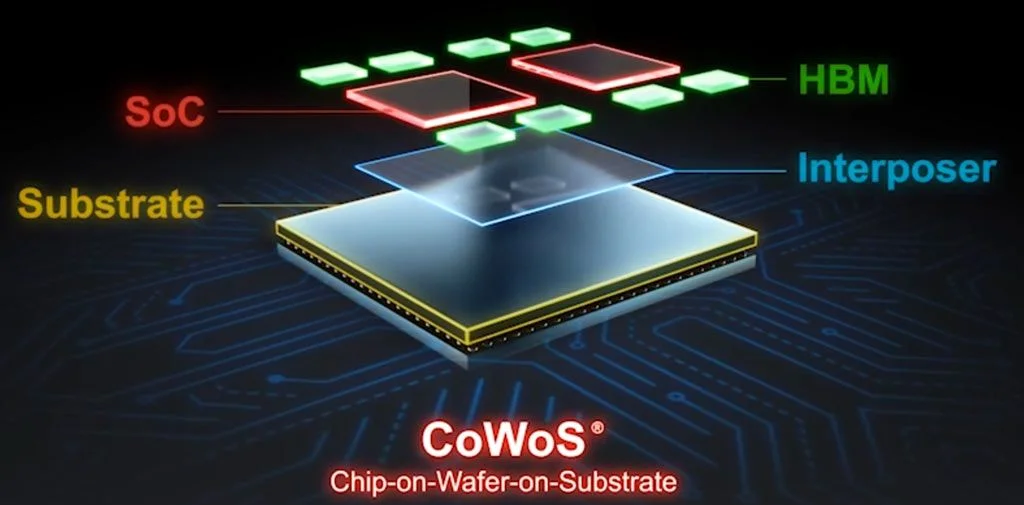
TSMC’s strategic announcement on May 14, 2026, serves as a definitive roadmap for the semiconductor industry’s role in the ongoing artificial intelligence revolution. By confirming the development of 18 new fabs and advanced packaging facilities across the globe, the Taiwanese giant is not merely expanding capacity; it is re-engineering the very architecture of AI hardware delivery. The focus on CoWoS (Chip on Wafer on Substrate) and SoIC (System on Integrated Chips) underscores a critical shift in semiconductor value—where the ‘back-end’ packaging process has become as technologically vital as the ‘front-end’ wafer fabrication.
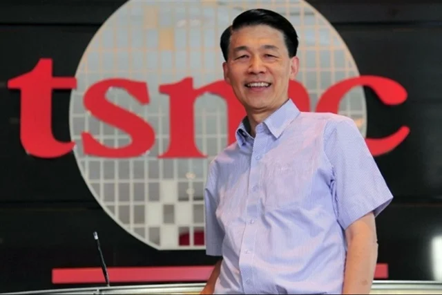
At the 2026 Technology Symposium, Vice President Bor-Zen Tien provided a technical deep dive into the integration of the 3DFabric platform with upcoming sub-2nm nodes. As AI models grow in complexity, the traditional monolithic chip design is reaching its thermal and economic limits. TSMC’s answer lies in heterogeneous integration.
Through SoIC, TSMC enables hybrid bonding with significantly higher interconnect density compared to traditional microbumps, facilitating the direct vertical stacking of logic and memory. This is crucial for the deployment of HBM4, where the proximity of memory to the processing unit dictates the overall bandwidth efficiency of AI accelerators like those produced by NVIDIA and AMD.
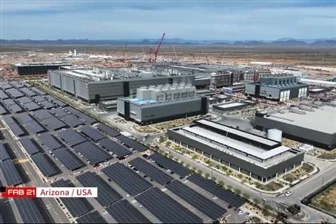
TSMC’s global expansion strategy, encompassing 18 new sites, is a masterclass in geopolitical and operational balancing. With active projects in Arizona (USA), Kumamoto (Japan), and Dresden (Germany), alongside its primary hubs in Hsinchu and Kaohsiung (Taiwan), TSMC is addressing the ‘Silicon Shield’ requirement of Western governments while maintaining its home-grown technical edge. This geographical diversification is complemented by the deployment of AI-powered smart manufacturing systems.
By utilizing massive data sets to train machine learning models that oversee plasma etching, lithography, and deposition, TSMC is targeting a ‘zero-defect’ manufacturing environment. This is particularly important for the A16 and N2P nodes, where the margin for error is measured in angstroms.
From an analyst’s perspective, this massive capital expenditure (CapEx) cycle reflects a strategic lock-in. By controlling the most advanced packaging standards (CoWoS-L and CoWoS-S), TSMC ensures that any designer wishing to utilize high-end memory or large-scale AI dies must remain within the TSMC ecosystem. The competitive moat is no longer just about who has the smallest transistor, but who can integrate the most diverse set of silicon components into a single, high-performance package.
As the industry moves toward 2027 and beyond, TSMC’s move to secure 18 new facilities ensures they remain the sole gatekeeper for the hardware that powers the next decade of digital transformation and sovereign AI initiatives. This expansion is a bold signal to competitors: TSMC is not just participating in the AI race; it is building the entire track.