🔍 Executive Summary
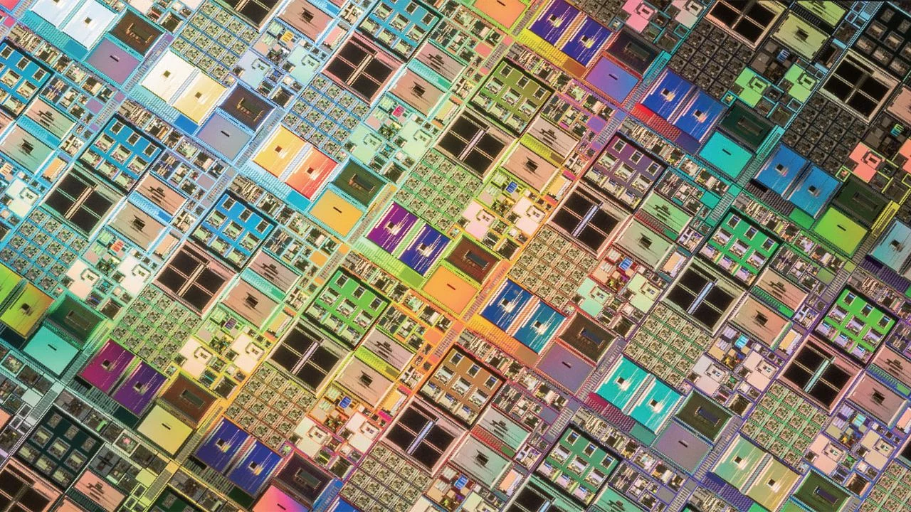
- As the semiconductor industry moves beyond the 2nm era, the leading foundries—TSMC, Intel, and Samsung—have unveiled divergent 1.4nm strategies. TSMC is emphasizing predictability through its A14 node, while Intel is taking an aggressive architectural gamble with its 14A process. Samsung is leveraging its early lead in Gate-All-Around (GAA) technology to focus on yield optimization. The race is now defined by the successful integration of High-NA EUV and backside power delivery systems.
Strategic Deep-Dive
The race toward the 1.4nm node has officially become the primary battleground for the semiconductor industry’s ‘Big Three’—TSMC, Intel, and Samsung. As we move beyond the 2nm era, the strategies of these giants are diverging in ways that reflect their differing internal cultures and market positions. From an analyst’s perspective, this divergence is not just about nanometers; it is a fundamental disagreement on the best technological path to overcome the limitations of photolithography and transistor physics.
Each player is betting billions on a specific combination of High-NA EUV adoption and advanced transistor architectures.
TSMC, the undisputed leader, is maintaining its ‘Predictability’ mantra. For TSMC, the transition to its A14 node is about providing a seamless evolutionary path for clients like Apple and NVIDIA. By focusing on process maturity and incremental reliability, TSMC minimizes the risk of production delays, which is paramount for high-volume consumer electronics.
TSMC’s strategy is to let its competitors take the pioneering risks with unproven architectures, while it perfects the manufacturing science required for global scale. This approach ensures that TSMC remains the safe bet for the world’s most critical silicon projects.
In contrast, Intel is executing a high-stakes ‘Architectural Shift’ with its 14A process. Intel is aggressively integrating PowerVia—its proprietary backside power delivery network (BSPDN)—and RibbonFET (its version of GAA) at a pace that rivals TSMC’s historical speed. Intel’s wager is that by moving the power delivery to the back of the wafer, it can significantly reduce voltage droop and increase logic density, effectively leapfrogging the performance metrics of its rivals.
Success here would mark a historic comeback for Intel Foundry Services (IFS), but the technical hurdles of coordinating these massive structural changes simultaneously are immense.
Samsung Foundry is centering its strategy on ‘Yield Optimization’ and leveraging its first-mover advantage in Gate-All-Around (GAA) technology. Having introduced GAA (MBCFET) at the 3nm node, Samsung has already faced the steep learning curve associated with this complex architecture. As it progresses toward 1.4nm, Samsung aims to capitalize on this experience to deliver superior yields compared to competitors who are only now transitioning to GAA.
For Samsung, the 1.4nm node is about proving that it can provide not just cutting-edge performance, but also the manufacturing consistency required to win back large-scale ASIC and mobile processor clients. As High-NA EUV lithography becomes the standard, the foundry that masters the intersection of yield, power delivery, and cost will define the next era of high-performance computing.