🔍 Executive Summary
- Singapore-based Galatek is leveraging AI-embedded automation to address critical yield bottlenecks in high-density, micron-level chip packaging.
- The startup is executing a dual-track expansion strategy, bridging the gap between Taiwan’s foundry expertise and Southeast Asia’s emerging semiconductor hubs.
- By focusing on the 'Back-end' supply chain, Galatek targets the most significant technical hurdle in scaling next-generation AI and HPC hardware.
Strategic Deep-Dive
Galatek, a high-growth Singaporean startup, is quickly becoming a critical player in the semiconductor ecosystem by focusing on one of the industry’s most pressing pain points: yield bottlenecks in advanced packaging. As the AI revolution demands increasingly large and complex chips—often requiring multiple dies to be integrated into a single package—the margin for error has shrunk to the micron level. Traditional automation tools, while precise, lack the real-time adaptive intelligence needed to handle the thermal and mechanical stresses that occur during the high-density bonding processes required for High-Performance Computing (HPC) hardware.
Galatek’s solution is a suite of AI-embedded equipment that utilizes deep learning models to predict and correct process deviations in real-time. By monitoring subtle environmental variables and mechanical vibrations, Galatek’s systems can adjust the packaging parameters ‘on the fly,’ significantly reducing the scrap rate of expensive AI silicon.
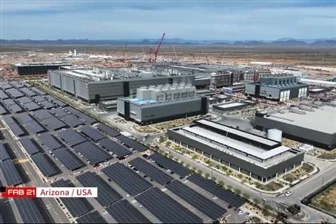
The technical significance of this cannot be overstated. We are currently witnessing a shift where Moore’s Law is being sustained not through front-end lithography alone, but through sophisticated ‘Back-end’ innovations like CoWoS (Chip on Wafer on Substrate) and HBM (High Bandwidth Memory) integration. These processes are inherently prone to yield issues due to their structural complexity.
Galatek’s ability to embed AI directly into the packaging hardware allows manufacturers to achieve industrial-scale throughput while maintaining laboratory-grade precision. This automation is the ‘missing link’ that allows OSAT (Outsourced Semiconductor Assembly and Test) providers to keep pace with the frantic delivery schedules demanded by AI hyper-scalers and GPU designers.
Geopolitically, Galatek’s dual-track expansion strategy is a masterclass in navigating the modern semiconductor landscape. By establishing deep ties with Taiwan’s foundries, Galatek gains access to the world’s most advanced manufacturing expertise and a concentration of the highest-value chip production. Simultaneously, its expansion into Southeast Asia taps into the burgeoning ‘China+1’ trend, where global tech giants are diversifying their supply chains away from single-country dependencies.
Countries like Malaysia, Singapore, and Vietnam are rapidly upgrading their OSAT capabilities, and Galatek’s AI-driven tools provide the technological leapfrog these regions need to compete with established hubs. This dual presence allows Galatek to serve as a bridge between the high-end innovation in Taiwan and the high-volume expansion in Southeast Asia. As the semiconductor industry enters an era where advanced packaging is the primary competitive differentiator, Galatek’s focus on micron-level automation and strategic geographic positioning makes it a formidable force in the race to scale the next generation of AI hardware.
The startup is effectively proving that in the AI age, the primary competitive advantage is no longer just the design of the chip, but the intelligence of the machine that builds it.