🔍 Executive Summary
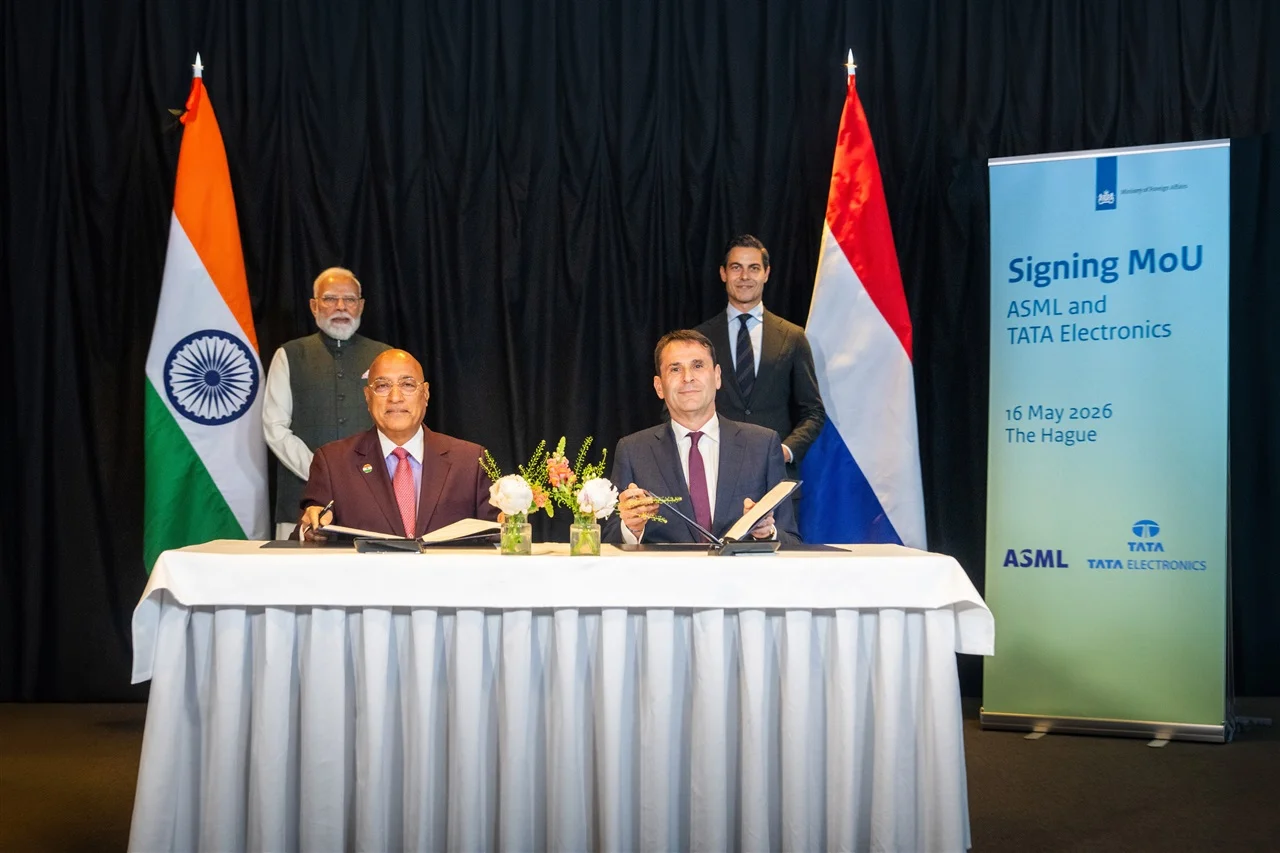
- Tata Electronics has solidified a landmark strategic partnership with ASML to catalyze the operational readiness of India's first 300mm semiconductor fabrication facility in Dholera, Gujarat. This high-level collaboration focuses on lithography technology transfer, equipment optimization, and workforce development, marking a decisive step in the Indian Semiconductor Mission (ISM) to secure a leading position in the global semiconductor value chain.
Strategic Deep-Dive
The strategic alliance between Tata Electronics and ASML marks a watershed moment in the global semiconductor landscape, signaling India’s formal entry into the high-stakes world of advanced semiconductor manufacturing. As part of a comprehensive Memorandum of Understanding (MOU), ASML—the world’s preeminent supplier of photolithography systems—will provide intensive technical support and operational expertise for Tata’s upcoming 300mm fabrication plant in Dholera, Gujarat. This facility is not merely a corporate asset but the flagship of the Indian Semiconductor Mission (ISM), a $10 billion government-backed initiative aimed at transforming the nation into a global electronics hub.
The transition to 300mm wafer technology is a complex industrial undertaking requiring extreme precision in lithography, an area where ASML’s involvement ensures that Tata can bypass many of the initial learning curve hurdles associated with large-scale fab operations.
From a technical perspective, the collaboration focuses on the critical ‘ramp-up’ phase, where the stability and yield of the production line are determined. ASML will assist in the installation and optimization of Deep Ultraviolet (DUV) and potentially future Extreme Ultraviolet (EUV) lithography tools, which are essential for producing the logic and memory chips that power modern AI and mobile devices. Furthermore, the partnership includes a robust framework for workforce development.
By establishing a knowledge bridge between the Netherlands and India, ASML will help train a new generation of Indian semiconductor engineers, addressing one of the most significant bottlenecks in the industry: the global talent shortage. This localized expertise will be crucial for maintaining the high uptime and precision required for sub-28nm manufacturing processes planned for the Dholera site.
Geopolitically, the Tata-ASML synergy is a major victory for the ‘China + 1’ strategy. As multinational corporations seek to diversify their manufacturing footprints away from concentrated risks in East Asia, India offers a politically stable and economically incentivized alternative. The Dholera Special Investment Region (DSIR) has been specifically prepared with dedicated water pipelines, high-load power grids, and logistics corridors to support this exact level of heavy industrial activity.
For ASML, the partnership opens a massive new market, securing a first-mover advantage in a region poised for exponential growth. For Tata and the Indian government, it provides the technological legitimacy required to attract other ecosystem players—such as chemical suppliers, wafer producers, and assembly-test houses—to the Gujarat cluster. Ultimately, this partnership serves as the bedrock for India’s long-term vision of technological self-reliance, moving the country from a consumer of global technology to a vital architect of the world’s digital infrastructure.