🔍 Executive Summary
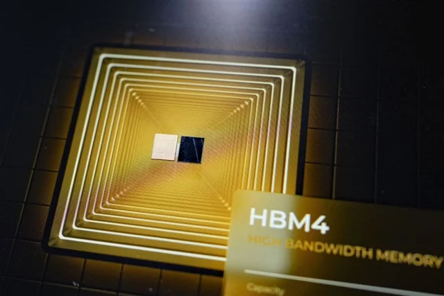
- TetraMem Inc., a high-tech disrupter headquartered in Silicon Valley, has announced a major breakthrough in the commercialization of non-Von Neumann architectures. The company has successfully completed the tape-out, fabrication, and initial silicon validation of its MLX200 platform. This system-on-chip (SoC) utilizes a 22nm multi-level RRAM (Resistive RAM) architecture to perform analog in-memory computing (IMC). This milestone is critical because it moves analog AI from theoretical modeling into a tangible, scalable silicon reality, offering a viable solution to the power-efficiency bottlene...
Strategic Deep-Dive
TetraMem Inc., a high-tech disrupter headquartered in Silicon Valley, has announced a major breakthrough in the commercialization of non-Von Neumann architectures. The company has successfully completed the tape-out, fabrication, and initial silicon validation of its MLX200 platform. This system-on-chip (SoC) utilizes a 22nm multi-level RRAM (Resistive RAM) architecture to perform analog in-memory computing (IMC).
This milestone is critical because it moves analog AI from theoretical modeling into a tangible, scalable silicon reality, offering a viable solution to the power-efficiency bottlenecks currently plaguing digital AI accelerators.
The core innovation of the MLX200 lies in its departure from the traditional Von Neumann architecture, where the constant shuffling of data between the CPU/GPU and the memory array creates a massive energy penalty known as the ‘Memory Wall.’ TetraMem’s analog IMC approach solves this by performing vector-matrix multiplication (VMM)—the fundamental operation for neural networks—directly within the memory cells. By leveraging the variable resistance states of RRAM, each cell can represent multiple bits of information and process them in the analog domain. While the industry has been racing toward 7nm and 5nm nodes for digital logic, TetraMem’s choice of the 22nm node for its RRAM implementation is a calculated strategic move.
The 22nm node offers a cost-effective balance, providing sufficient precision for analog signals and robust endurance for RRAM cells, while avoiding the exorbitant design costs of sub-10nm fabrication. This makes it an ideal candidate for high-volume edge AI applications where cost-per-unit is as critical as energy efficiency.
The implications for the edge AI market are profound. Devices that require persistent ‘Always-on’ intelligence, such as smart cameras, industrial IoT sensors, and biometric wearables, have long been hindered by the battery life constraints of digital SoCs. The MLX200 offers a performance-per-watt advantage that is orders of magnitude higher than conventional digital solutions.
As the industry shifts toward decentralized AI, where processing occurs at the source rather than in the cloud, TetraMem’s analog IMC technology provides the necessary blueprint for ultra-low-power, high-throughput intelligence. With successful silicon validation in hand, TetraMem is now positioned to lead the market transition toward energy-efficient, analog-driven AI, bridging the gap between sophisticated neural networks and the practical power constraints of the physical world. The next phase involves ecosystem integration and full-scale production to meet the rising demand for efficient edge intelligence.