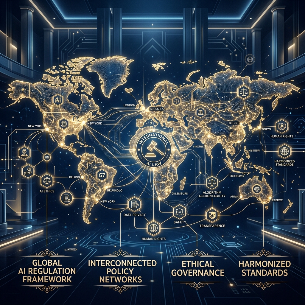
🔍 Executive Summary
- Asia Electric Material (AEM), a leading specialist in Flexible Copper Clad Laminate (FCCL) technology, has announced a significant operational shift that marks the culmination of years of rigorous R&D. For fiscal year 2026, the company is pivoting its focus toward global product promotion and the critical phase of customer sample certification. This transition is specifically engineered to address the escalating requirements of the semiconductor and artificial intelligence (AI) application markets, where conventional materials are increasingly failing to meet the thermal and electrical demands...
Strategic Deep-Dive
The Strategic Evolution of Advanced Semiconductor Materials
Asia Electric Material (AEM), a leading specialist in Flexible Copper Clad Laminate (FCCL) technology, has announced a significant operational shift that marks the culmination of years of rigorous R&D. For fiscal year 2026, the company is pivoting its focus toward global product promotion and the critical phase of customer sample certification. This transition is specifically engineered to address the escalating requirements of the semiconductor and artificial intelligence (AI) application markets, where conventional materials are increasingly failing to meet the thermal and electrical demands of next-generation hardware architectures.
Technical Deep Dive: PTFE and Structural Stability Solutions
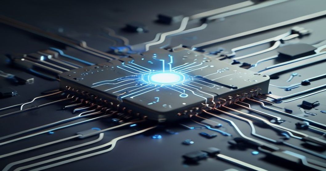
AEM’s product roadmap is anchored by two breakthrough categories: PTFE (Polytetrafluoroethylene) materials and anti-warpage films. From a data architect’s perspective, the move toward PTFE is a necessity driven by the rise of 800G and 1.6T networking standards. PTFE offers an exceptionally low dielectric loss tangent, which is vital for maintaining signal integrity at high frequencies.
As AI clusters demand higher throughput and lower latency, the dielectric properties of the substrate become a bottleneck. AEM’s PTFE-based solutions enable lower insertion loss, ensuring that high-speed signals between GPUs and memory modules remain clear and consistent, effectively pushing the boundaries of high-frequency communication.
In tandem with electrical performance, AEM is tackling the physical challenges of modern packaging through its anti-warpage and heat-dissipation films. As semiconductor packages transition to heterogeneous integration and large-area substrates (such as those used in CoWoS packaging), the Coefficient of Thermal Expansion (CTE) mismatch between different materials often leads to substrate warping during the soldering process. This warping causes micro-cracks and interconnect failures, drastically reducing manufacturing yields.
AEM’s anti-warpage film provides a robust mechanical counterforce and enhanced thermal conductivity, stabilizing the substrate during high-temperature cycles. This not only improves the reliability of AI accelerators but also directly impacts the bottom line of semiconductor manufacturers by enhancing production yields.
Future Outlook: Building a Resilient AI Supply Chain
As AEM enters the 2026 certification cycle, it is positioning itself as a mission-critical partner for global tech giants and leading OSAT (Outsourced Semiconductor Assembly and Test) providers. The successful validation of these materials will signal a move away from the commoditized FCCL market into a high-margin, specialized niche. For the broader industry, AEM’s entry provides a much-needed diversification in the supply of high-performance electronic materials.
By securing certification from major semiconductor clients, AEM will likely become a linchpin in the AI hardware ecosystem, supporting the infrastructure that powers everything from Large Language Models (LLMs) to autonomous edge devices. The company’s focus on material-level innovation serves as a foundational layer for the next decade of computing progress, where the physical limits of materials are the new frontier of Moore’s Law.