🔍 Executive Summary
- Samsung Electronics has reportedly achieved a major breakthrough in 1b DRAM yields, a move that significantly enhances its manufacturing capacity for AI-centric High Bandwidth Memory and addresses market skepticism regarding its technical execution.
Strategic Deep-Dive
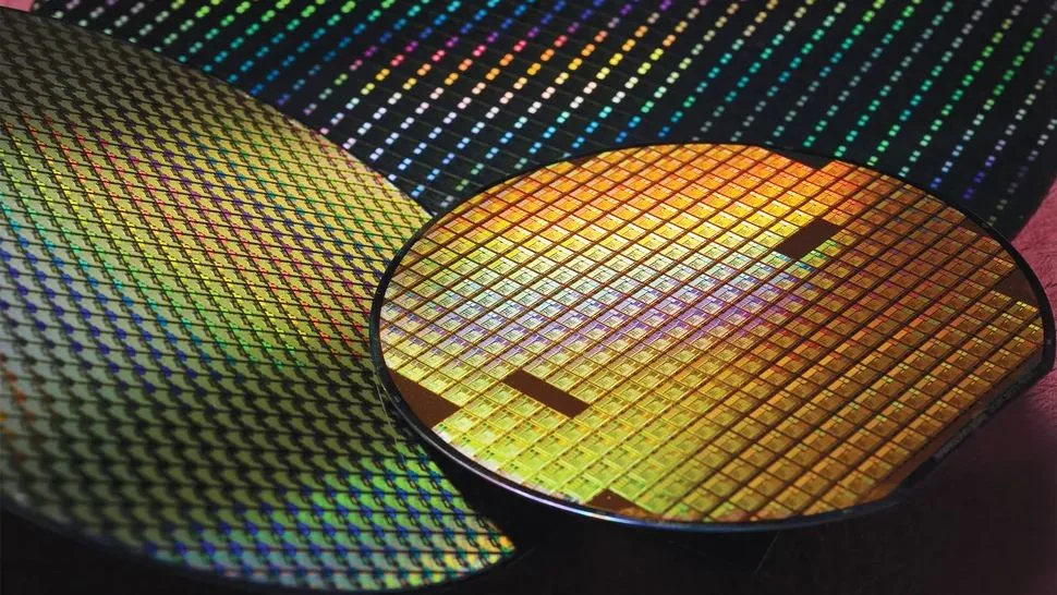
Samsung Electronics is signaling a major offensive in the AI memory market through a reported breakthrough in its 1b (12nm-class) DRAM manufacturing yields. As the primary building block for High Bandwidth Memory (HBM), the success of the 1b node is non-negotiable for any memory maker aiming to lead the generative AI era. HBM production is notoriously complex, involving the vertical stacking of multiple DRAM dies connected via Through-Silicon Vias (TSV).
In this architecture, a single defective die can ruin an entire HBM stack, making ‘Known Good Die’ (KGD) yields the primary battleground for profitability. Samsung’s progress in stabilizing 1b yields suggests that its investments in Extreme Ultraviolet (EUV) lithography and advanced material science are finally reaching a point of high-volume efficiency. This development is strategically timed to address the supply-constrained environment of the AI accelerator market.
While NVIDIA and AMD remain the dominant off-takers of high-end HBM (according to market consensus), their selection of suppliers hinges on ‘Yield-to-Scale’—the ability to deliver millions of units with consistent thermal and electrical profiles. Samsung’s improved yield translates directly into a more competitive cost structure and, more importantly, a higher ‘Thermal Dissipation Envelope’ for its finished HBM3e and upcoming HBM4 modules. Architecturally, the 1b node provides the necessary density and power efficiency to meet the stringent requirements of next-generation AI servers.
For Samsung, which has faced intense competition and scrutiny over its HBM roadmap, this yield improvement is a powerful technical rebuttal. It allows the company to leverage its massive manufacturing footprint to flood the market with high-quality components, potentially shifting the pricing power back in its favor. As the industry moves toward the HBM4 era, where custom logic integration will become more prevalent, having a rock-solid, high-yield 1b foundation is the essential first step.
Samsung’s manufacturing prowess is once again being deployed as its primary strategic weapon, aiming to solve the memory bottleneck that currently constrains global AI compute capacity while maintaining healthy operating margins in a capital-intensive sector.