🔍 Executive Summary
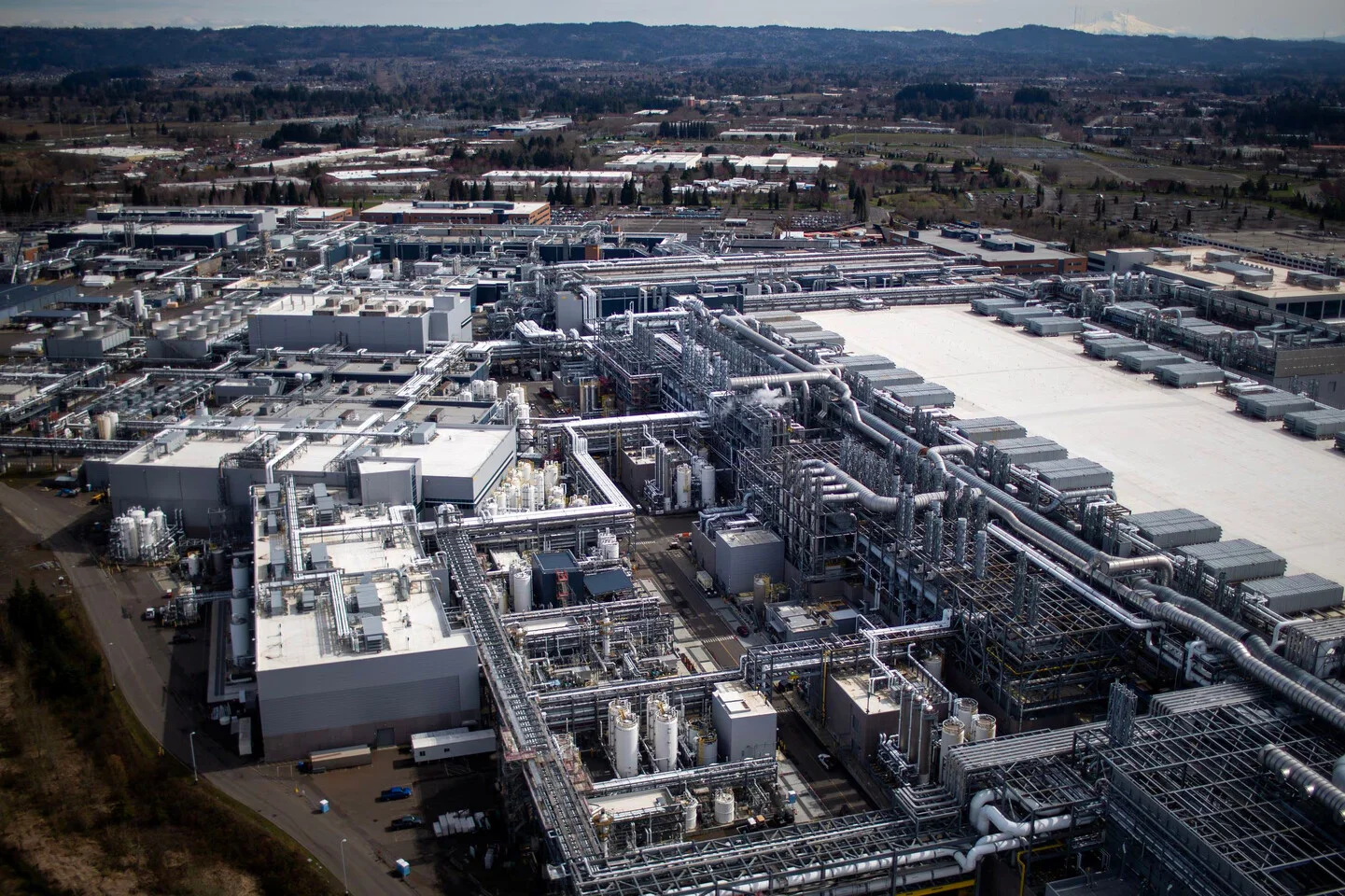
- The VLSI 2025 conference has served as a critical nexus for semiconductor innovation, revealing the technical and economic roadmaps for the sub-2nm era. A primary focus was the detailed breakdown of Intel 18A, providing a rare look at the manufacturing cost structures that will determine the viability of Intel’s foundry ambitions. As the industry moves toward mass production on these advanced nodes, the economic efficiency of gate-all-around (GAA) architectures becomes as important as their performance benchmarks. The technical program also highlighted significant advancements in logic transis...
Strategic Deep-Dive
The VLSI 2025 conference has served as a critical nexus for semiconductor innovation, revealing the technical and economic roadmaps for the sub-2nm era. A primary focus was the detailed breakdown of Intel 18A, providing a rare look at the manufacturing cost structures that will determine the viability of Intel’s foundry ambitions. As the industry moves toward mass production on these advanced nodes, the economic efficiency of gate-all-around (GAA) architectures becomes as important as their performance benchmarks.
The technical program also highlighted significant advancements in logic transistors and interconnects, notably featuring China’s FlipFET and new strategies for signal routing density.
A recurring theme was the strategic pivot toward Backside Power Delivery, a technology that separates power routing from signal routing to reduce IR drop and increase transistor density. In the memory space, the debate intensified over the future of DRAM; architects are weighing the evolutionary 4F2 cell structure against the revolutionary leap to 3D DRAM to bypass traditional scaling limits. Beyond individual transistors, the most significant conceptual shift introduced was the ‘Atoms to Fabs’ digital twin paradigm.
By creating hyper-accurate digital replicas that simulate everything from atomistic material interactions to whole-factory logistics, manufacturers are aiming to slash the time-to-market for complex nodes. This fusion of software-defined manufacturing and advanced lithography represents the only sustainable path forward as physical scaling hits diminishing returns. For the industry, VLSI 2025 confirmed that the future of high-performance computing will be built on a foundation of simulation-driven manufacturing and radical power-delivery innovations.