🔍 Executive Summary
- Intel has expanded its long-term semiconductor roadmap by initiating the development of 10A and 7A nodes for the 2030s, while preparing a critical PDK release for its 14A node to secure foundry partners.
Strategic Deep-Dive
Intel has formally initiated the development of its 10A (1nm) and 7A (0.7nm) process nodes, marking a defiant step toward reclaiming semiconductor leadership in the 2030s. This announcement clarifies the company’s long-term trajectory, moving beyond the 14A (1.4nm) node which is currently the cornerstone of its IDM 2.0 strategy. By outlining a roadmap that extends into the next decade, Intel is attempting to provide a predictable cadence of technological innovation for a foundry market that is increasingly wary of single-source dependencies on TSMC.
The transition to the ‘Angstrom era’ represents more than just a nomenclature shift; it signifies a fundamental overhaul of semiconductor physics and manufacturing logistics.
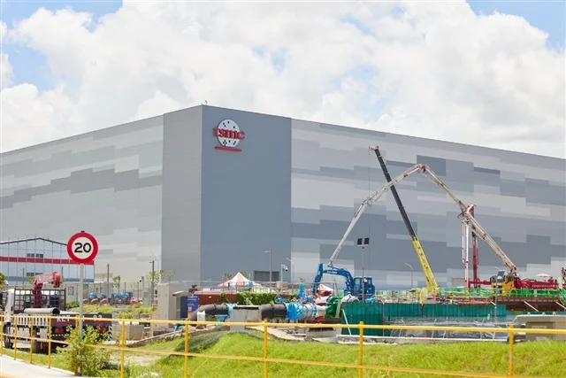
The immediate focus for the industry, however, remains on the 14A node, which is slated for high-volume manufacturing (HVM) in 2029. Intel has confirmed that the 14A process remains on schedule, with a pivotal milestone approaching this October: the release of the version 1.0 Process Design Kit (PDK). For fabless customers like NVIDIA, Broadcom, and AWS, the PDK is the essential bridge between architectural design and physical silicon.
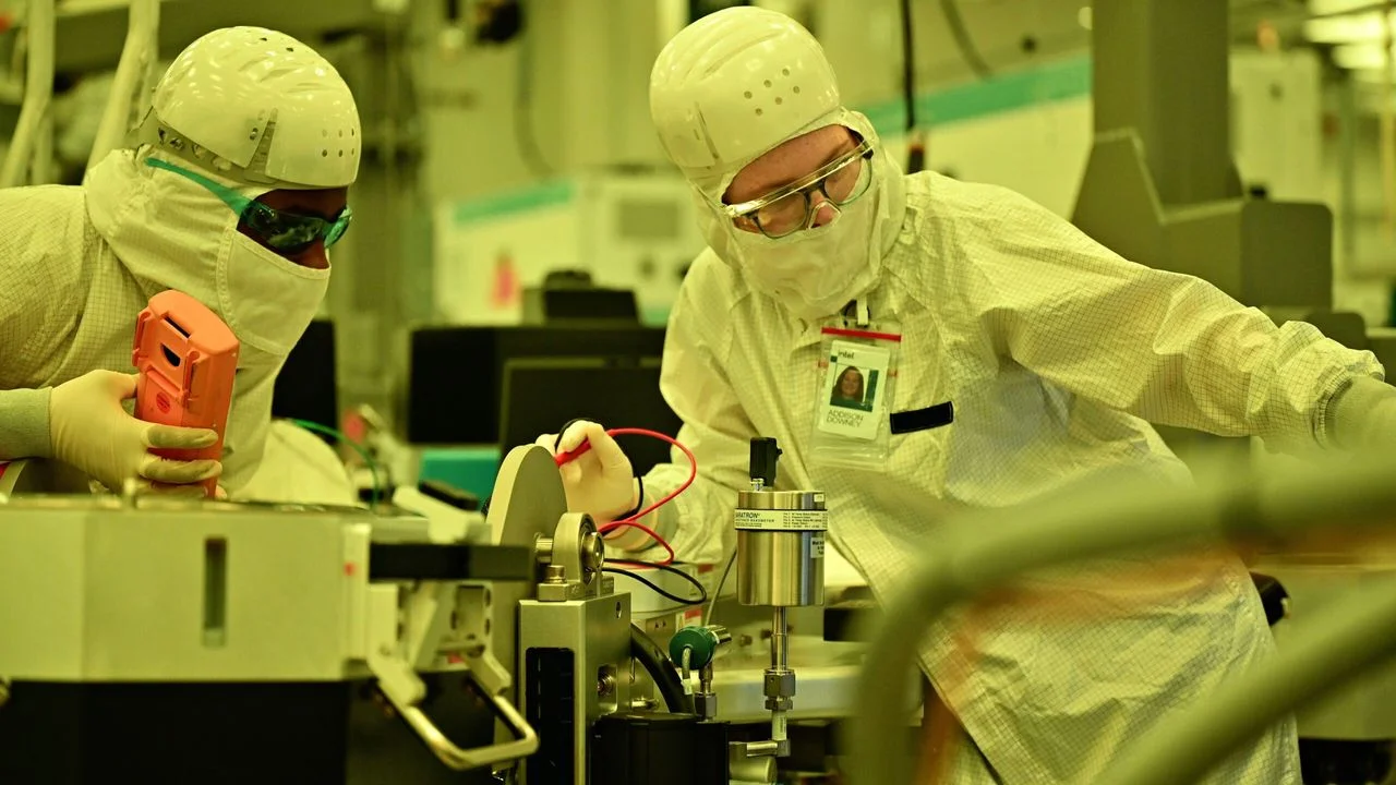
A timely and robust PDK release will serve as a ‘moment of truth’ for Intel Foundry Services (IFS), demonstrating that the company can maintain operational discipline and deliver the software tooling necessary for third-party designers to optimize their chips for Intel’s specific gate-all-around (GAA) implementation, known as RibbonFET.
To achieve the densities required for 10A and 7A, Intel is betting heavily on its early adoption of High-NA (Numerical Aperture) EUV lithography. These advanced machines, costing over $350 million each, are necessary to pattern the incredibly fine features of sub-1nm nodes without resorting to complex and yield-killing multi-patterning techniques. Alongside High-NA EUV, Intel is integrating PowerVia—a backside power delivery solution that decouples power routing from signal routing, significantly reducing cell area and improving performance.
The technical competition is fierce; TSMC’s A16 node and Samsung’s 1.4nm roadmap are direct rivals to Intel’s 14A. By starting development on 10A and 7A now, Intel aims to leapfrog the competition in transistor density and energy efficiency. However, the financial stakes are astronomical.
The capital intensity of these ‘Angstrom-era’ fabs requires a massive and consistent customer base to reach break-even yields. Intel’s strategy is clear: provide a decade-long vision of technological superiority to lure the world’s largest chip designers away from their incumbents and into the Intel ecosystem. As the company moves toward the October PDK release, the semiconductor world will be watching to see if Intel’s execution can finally match its ambitious rhetoric.