🔍 Executive Summary
- Samsung Electronics is intensifying its push into silicon photonics with new foundry services and pilot production, aiming to challenge TSMC's established lead. While Samsung focuses on aggressive investment, TSMC’s COUPE technology and its robust ecosystem of domestic partners remain a high barrier to entry in the burgeoning CPO market.
Strategic Deep-Dive
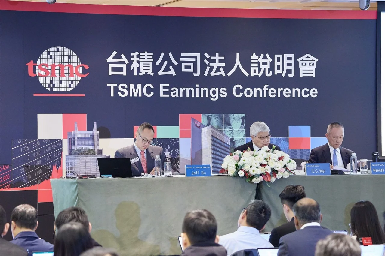
The battle for dominance in the next generation of optical communications is intensifying as Samsung Electronics and TSMC go head-to-head in the silicon photonics arena. Silicon photonics, which integrates lasers and optical components directly onto silicon substrates, is the foundational technology required for Co-Packaged Optics (CPO), the industry’s answer to the bandwidth limitations of electrical I/O. During its latest earnings call, Samsung signaled its readiness to take on this challenge by launching specialized foundry services and entering the pilot production phase for advanced optical communication modules.
Supported by aggressive capital expenditure, Samsung aims to fast-track these modules into mass production, leveraging its unique status as a total solution provider capable of manufacturing both high-bandwidth memory and logic chips in-house.
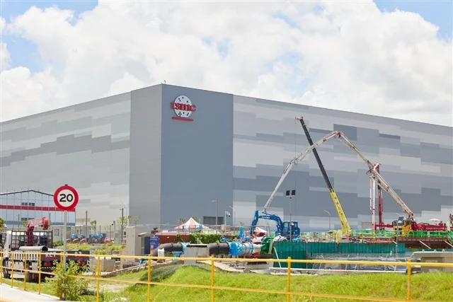
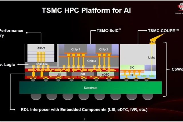
However, Samsung faces a formidable opponent in TSMC, which has already established a significant multi-year lead in this space. TSMC’s COUPE (Compact Universal Photonic Engine) technology represents the current gold standard in optical integration. COUPE utilizes advanced 3D packaging to stack photonic integrated circuits (PICs) directly onto electronic integrated circuits (EICs), offering superior performance in terms of signal loss, power efficiency, and physical footprint.
Beyond the technical specifications, TSMC’s greatest competitive advantage is the ‘Taiwan Ecosystem.’ Silicon photonics is not a standalone process; it requires a high degree of synchronized collaboration between chip designers, foundries, and packaging houses. TSMC has successfully integrated its advanced packaging technologies, such as CoWoS (Chip on Wafer on Substrate), with its optical engines, supported by a vast network of domestic partners that handle everything from substrate manufacturing to specialized testing.
Samsung’s catch-up strategy involves utilizing its internal synergies to provide a more integrated offering, but the company must overcome the head start TSMC has in ecosystem maturity. For customers in the AI and high-performance computing (HPC) sectors, the reliability and yield of the entire supply chain are just as important as the raw performance of the individual silicon photonics chip. TSMC’s proven track record and its COUPE platform provide a level of supply chain security that Samsung is now working hard to replicate.
As the industry prepares for the transition to 1.6T networking and eventually 3.2T architectures, the rivalry between these two foundry giants will determine the global standard for how light and silicon are integrated into the heart of the world’s most powerful compute nodes. The success of Samsung’s foundry ambitions in this space will depend on its ability to build a comparable partner ecosystem that can offer the same ‘plug-and-play’ convenience and yield assurance that TSMC’s established partners currently provide to the market’s biggest players.