🔍 Executive Summary
- Researchers at Fraunhofer IPMS have pioneered a wafer-level integration method using 'Silicon Pockets' to fuse chiplets seamlessly. This technique drastically reduces Z-height and interconnect complexity compared to traditional 2.5D interposer-based solutions.
Strategic Deep-Dive
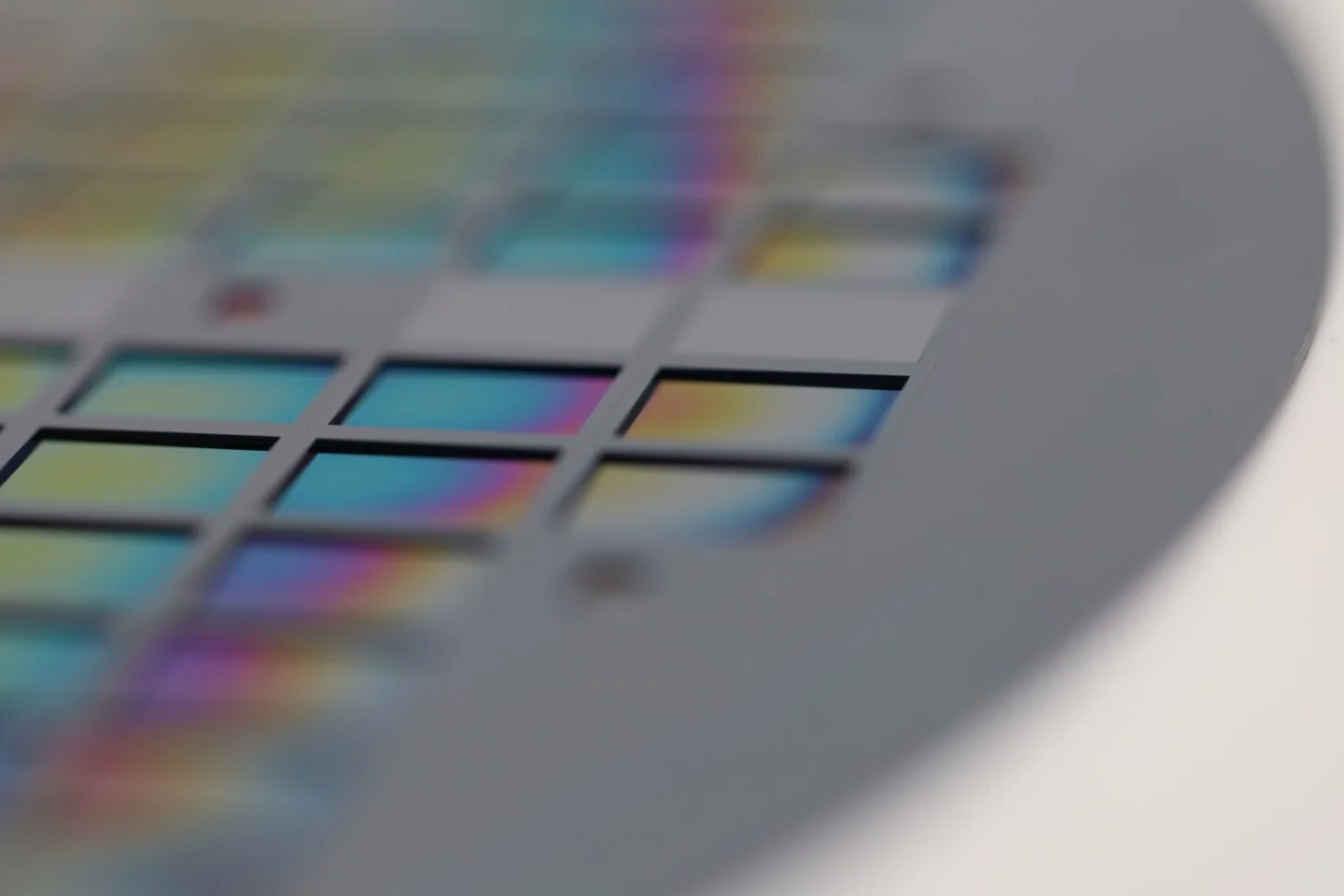
The Fraunhofer IPMS breakthrough in wafer-level chiplet integration introduces the ‘Silicon Pocket’ methodology, a technique that challenges the dominance of traditional 2.5D and 3D packaging. By embedding chiplets into pre-structured pockets within a silicon wafer, this method achieves a level of interconnect density and structural integrity that mimics a monolithic die. This is a significant leap forward for the European APECS pilot line, providing a scalable alternative to interposer-based integration.
Technically, the Silicon Pocket approach offers superior advantages in Z-height and thermal management. Traditional 2.5D solutions, such as TSMC’s CoWoS or Intel’s EMIB, rely on intermediate layers or bridges that add vertical bulk and introduce thermal resistance. Fraunhofer’s method allows chiplets to sit flush within the substrate, enabling a shorter thermal path to the cooling solution and reducing the parasitic capacitance associated with long interconnects.
This ‘seamless fusion’ minimizes signal latency between logic and memory components, which is critical for the next generation of AI accelerators and high-performance edge computing units. By integrating disparate nodes at the wafer level, manufacturers can maintain high yields while achieving the performance density of a single-chip solution.


