🔍 Executive Summary
- India's semiconductor strategy is evolving into its second phase, pivoting from initial capital-intensive fab attraction to a sophisticated focus on ecosystem sustainability by addressing 'weak links' in OSAT, design, and specialized supply chains.
Strategic Deep-Dive
The India Semiconductor Mission (ISM) is undergoing a fundamental recalibration as it transitions into Phase 2.0. While the inaugural phase was characterized by a massive push to secure commitments for semiconductor fabrication units (fabs) and Outsourced Semiconductor Assembly and Test (OSAT) facilities through lucrative financial incentives, the second phase shifts the focus toward the structural integrity of the ecosystem. As a senior technology correspondent, I observe this as a transition from ‘attracting investments’ to ‘building a sustainable industrial engine.’ The Indian government is now confronting the reality that a few isolated fabs do not constitute a semiconductor superpower; rather, they require a dense, interconnected web of suppliers, designers, and specialized service providers.
At the heart of ISM 2.0 is the mandate to fix ‘five weak links’ identified by industry experts and policymakers. These include high-end semiconductor design, advanced packaging technologies, the domestic supply of semiconductor-grade chemicals and gases, specialized equipment maintenance, and a robust pipeline of VLSI (Very Large Scale Integration) talent. From a data systems architecture perspective, the lack of a domestic design ecosystem means that India remains a contract manufacturer rather than an IP (Intellectual Property) holder.
By incentivizing design firms, India aims to capture the higher end of the value chain, ensuring that the chips fabricated on its soil are also conceived there. This creates a feedback loop that drives innovation and long-term economic resilience.
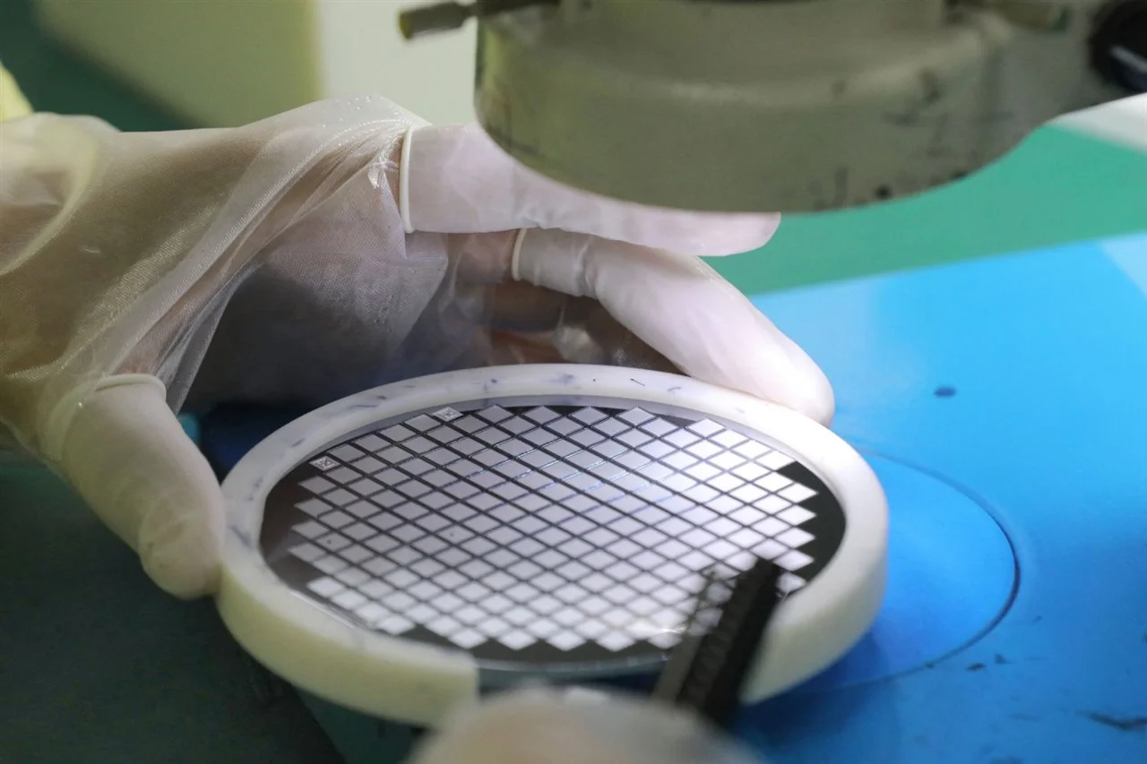
Furthermore, the focus on OSAT and advanced packaging is strategic. In the current era of heterogenous integration, where performance gains are increasingly driven by how chips are packaged rather than just how small the transistors are, India’s investment in these ‘back-end’ processes is critical. Without sophisticated domestic OSAT capabilities, India would be forced to ship its unfinished silicon abroad for testing and assembly, adding significant costs and security risks to the supply chain.
ISM 2.0 seeks to mitigate this by fostering local partnerships that can handle the complexity of modern multi-die architectures.
The mission also addresses the ‘hidden’ logistics of semiconductor manufacturing—the ultra-pure water, specialized gases, and chemicals required for production. Establishing a domestic supply chain for these materials is a massive undertaking that requires stringent environmental controls and chemical engineering expertise. By tackling these foundational issues, ISM 2.0 is attempting to lower the Total Cost of Ownership (TCO) for global players considering India as an alternative to existing hubs in East Asia.
The success of this pivot will determine whether India’s semiconductor ambitions are a fleeting policy trend or the birth of a global hardware powerhouse that can withstand the pressures of geopolitical shifts and technological disruptions for decades to come.