🔍 Executive Summary
- SK Hynix is repurposing its Cheongju mask fab to prioritize wafer testing and HBM packaging, addressing critical back-end bottlenecks.
- The shift highlights a massive industry transition where advanced packaging yield is becoming the primary differentiator in AI memory.
- With HBM4 on the horizon, the focus has moved to solving the 'Known Good Die' (KGD) challenge and managing complex thermal profiles.
Strategic Deep-Dive
The global semiconductor landscape is witnessing a profound paradigm shift where the traditional dominance of front-end lithographic scaling is being challenged by the critical importance of back-end packaging and testing. SK Hynix’s strategic decision to pivot its Cheongju campus operations toward wafer testing and High-Bandwidth Memory (HBM) packaging serves as a definitive marker of this industry-wide transition. As the demand for AI-specific memory continues its exponential climb, the technical bottleneck has fundamentally shifted from transistor density to the efficiency and reliability with which multiple dies can be integrated and validated within a three-dimensional architecture.
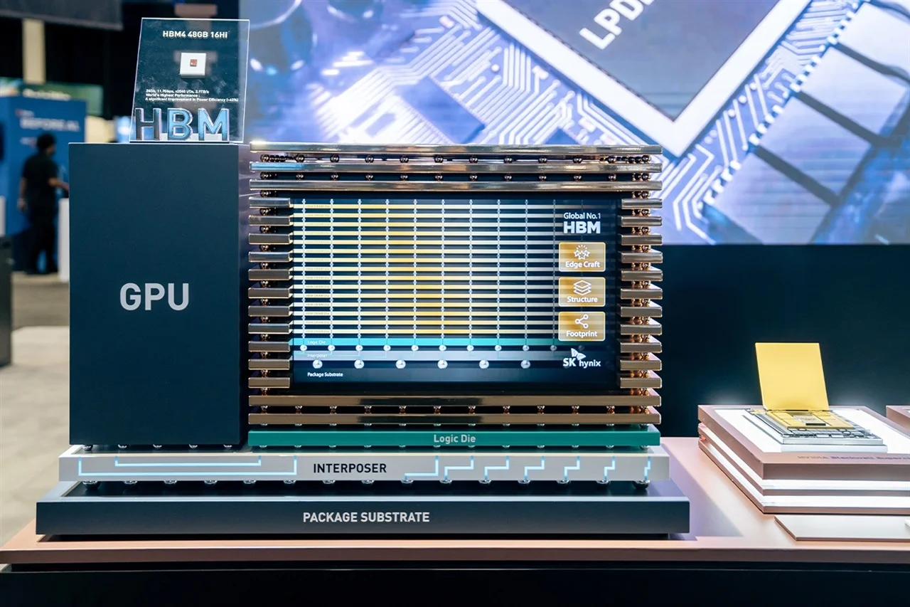
HBM, the indispensable backbone of modern AI accelerators, necessitates a manufacturing flow that is exponentially more complex than standard DRAM. The process involves high-density Through-Silicon Via (TSV) technology and sophisticated multi-die stacking that pushes the limits of material science. Unlike commodity memory, the cumulative yield loss in HBM is statistically unforgiving; this is known as the ‘Known Good Die’ (KGD) problem.
In a 12-layer or the upcoming 16-layer HBM4 stack, a single defective die renders the entire unit useless. Consequently, the industry is experiencing intense ‘Back-end Pressure’ where the final stages of production—high-speed testing, precision bonding, and thermal management—become the primary determinants of a manufacturer’s profit margin. By repurposing the Cheongju mask fab for these specific tasks, SK Hynix is signaling that yield optimization at the wafer and stack level is now a higher strategic priority than the production of legacy masks.
Technically, this shift involves moving beyond traditional mass reflow processes toward advanced Thermal Compression Bonding (TCB) and even hybrid bonding for next-generation HBM4. Hybrid bonding, which eliminates the need for solder bumps by connecting copper pads directly, requires an ultra-clean environment comparable to front-end fabs. This explains why SK Hynix is retooling existing high-end fab space rather than building low-specification assembly lines.
Furthermore, the physical proximity of high-end testing facilities to the main fabrication lines is a logistical necessity for rapid feedback loops. Historically, packaging was viewed as a low-margin commodity service. However, in May 2026, advanced packaging is the new ‘Moore’s Law.’ The ability to perform high-precision wafer testing before and during the stacking process is what separates the leaders from the laggards in the AI hardware war.
This strategic reconfiguration at the Cheongju campus is an architectural commitment to maintaining a dominant position as the preferred supplier for NVIDIA and other global AI giants, ensuring that innovation is measured by the integrity of the stack and the precision of the test.


