🔍 Executive Summary
- AMD's Strix Halo architecture marks a pivotal shift toward silicon disaggregation, leveraging chiplet-based design to deliver discrete-level graphical performance within a thermally optimized and yield-efficient mobile processor package.
Strategic Deep-Dive
The emergence of AMD’s Strix Halo represents a sophisticated response to the plateauing gains of Moore’s Law and the escalating complexities of monolithic semiconductor fabrication. As a Senior Information Architect might observe, the industry has reached a ‘reticle limit’ where cramming more transistors onto a single piece of silicon leads to diminishing economic returns and thermal management nightmares. Strix Halo addresses this by embracing the disaggregation of compute resources, moving the Accelerated Processing Unit (APU) from a single-die constraint into a multi-die ‘System-in-Package’ (SiP) philosophy.
This shift is not merely an incremental upgrade but a fundamental re-engineering of how mobile silicon interacts with its environment and its workloads.
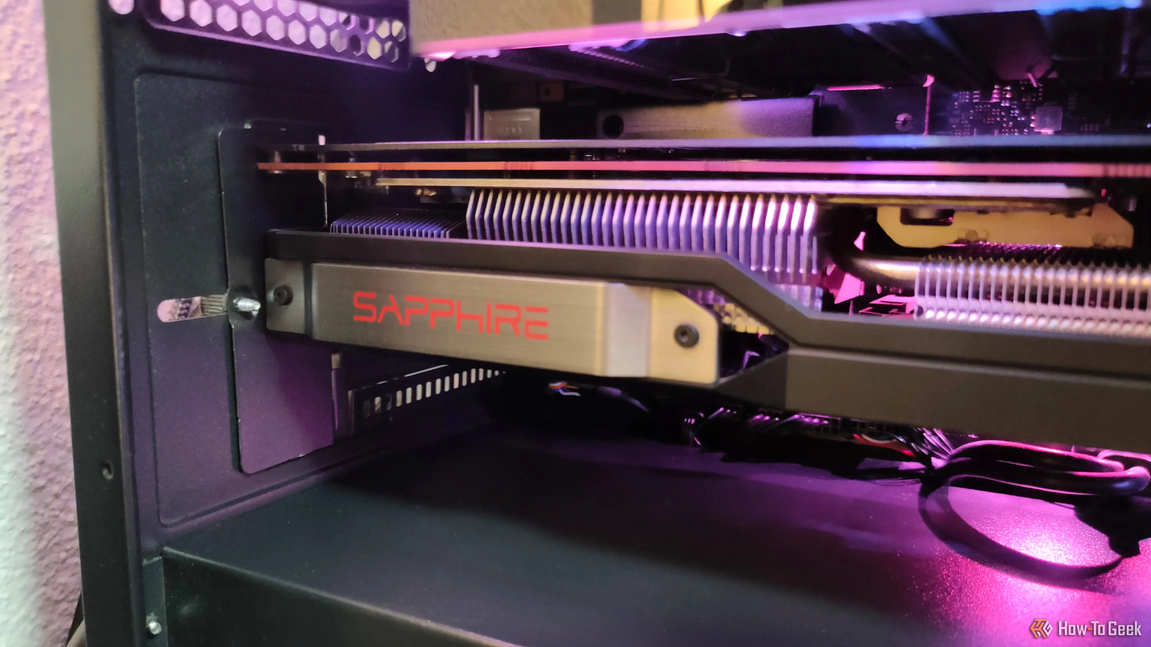
At the technical heart of the Strix Halo architecture lies the strategic separation of the CPU and GPU logic into discrete chiplets. In a traditional monolithic design, the proximity of high-frequency CPU cores to a massive GPU array creates a concentrated thermal envelope, often forcing aggressive power throttling to prevent hardware degradation. By decoupling these components, AMD can optimize the thermal floor of each chiplet independently.
This disaggregation allows for the inclusion of a significantly larger GPU component than was previously feasible in a shared-die environment. This is critical for modern ‘prosumer’ applications—ranging from AI-driven creative suites to real-time rendering—which demand sustained high-performance throughput that integrated solutions historically could not provide without severe performance drop-offs.
Furthermore, the Strix Halo approach optimizes the economic lifecycle of silicon production. Manufacturing smaller, specialized chiplets yields significantly higher rates of functional silicon compared to large, monolithic dies where a single defect can render the entire chip unusable. This manufacturing efficiency translates into a more competitive price-to-performance ratio for premium mobile devices.
From an architectural standpoint, the interconnect fabric linking these chiplets is the unsung hero, providing the low-latency, high-bandwidth communication necessary to make the split-die configuration feel like a single, cohesive processor to the operating system.
For the broader technology market, Strix Halo signals the ‘SaaS-ification’ of hardware design—where modularity and scalability become the primary drivers. Original Equipment Manufacturers (OEMs) can now rethink the industrial design of laptops. By removing the need for a secondary discrete GPU and its associated voltage regulator modules (VRMs) and expansive cooling assemblies, engineers can reclaim internal volume for larger batteries, improved audio chambers, or more robust structural reinforcement.
In essence, the Strix Halo architecture is AMD’s bid to monopolize the high-end mobile segment by offering a ’no-compromise’ silicon solution that matches discrete performance with integrated efficiency, effectively marking the beginning of the end for entry-to-mid-level discrete mobile GPUs.