🔍 Executive Summary
- As AI chips move toward more complex multi-die architectures, the industry is hitting a new bottleneck: ABF substrates. This critical packaging material is now the primary factor limiting the production of high-end GPUs and networking ASICs.
Strategic Deep-Dive
In the complex hierarchy of semiconductor manufacturing, the spotlight is shifting from the front-end brilliance of lithography to the back-end necessity of substrate materials. Specifically, Ajinomoto Build-up Film (ABF) substrates have emerged as the primary bottleneck in the AI hardware supply chain. As a data systems architect, it is clear that while we focus on TFLOPS and memory bandwidth, the physical interconnect layer—the ABF substrate—is where the current AI expansion is being throttled.
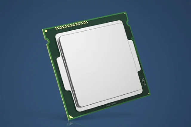
These substrates are not merely carriers; they are the electrical nervous system that facilitates high-speed communication between logic dies, HBM stacks, and the system board.
The surge in demand for AI-centric CPUs, GPUs, and custom ASICs has fundamentally altered the technical requirements of these substrates. Modern AI processors increasingly rely on ‘chiplet’ architectures and heterogenous integration (like CoWoS), which demand significantly larger substrate surface areas and higher layer counts—often exceeding 20 layers. This complexity introduces immense manufacturing challenges.
Larger substrates are more prone to warping during the thermal cycles of the assembly process, and finer circuit patterns within the layers increase the probability of shorts or opens. Consequently, the industry is seeing a paradox where manufacturing capacity is being added, but ’effective capacity’ remains low due to yield losses associated with these advanced specifications.
Moreover, the chemical composition of the insulation material itself—the ABF film—is a single-source dependency. Developed by Japan’s Ajinomoto Co., this specialized resin is prized for its low expansion and excellent insulation properties at high frequencies. Any disruption in the production of this film or a failure by substrate makers (like Unimicron, Ibiden, or Nan Ya) to improve their build-up processes directly impacts the shipment of high-end networking chips and AI accelerators.
For cloud service providers and hyperscalers, this means that even if NVIDIA or AMD has the silicon, the lack of a substrate can delay the deployment of entire data center racks by months.
From a strategic standpoint, the ABF substrate crisis highlights the fragility of the ‘advanced packaging’ moat. As Moore’s Law slows at the transistor level, the industry is squeezing performance out of the package, making the substrate a high-value, high-risk component. Companies that have secured long-term supply agreements or have invested in vertical integration of their packaging pipeline are finding themselves with a massive competitive advantage.
Looking forward, the development of alternative glass substrates or new organic materials may eventually ease the strain, but for the immediate future, ABF remains the gatekeeper of the AI revolution. Architects must now account for substrate lead times as a critical path in their infrastructure planning.