🔍 Executive Summary
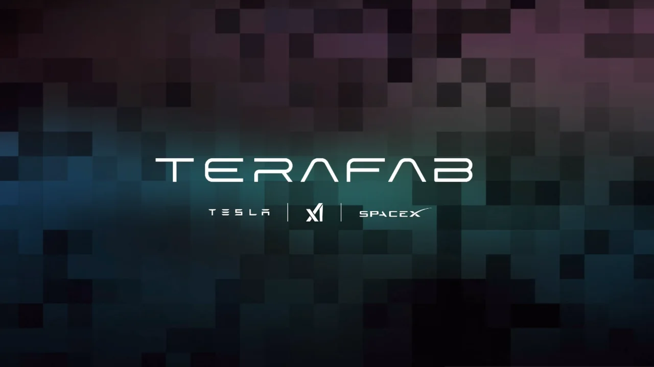
- ASML CEO Christophe Fouquet has officially confirmed engagement in high-level discussions with Elon Musk concerning the ambitious 'TeraFab' project. With a projected investment of $119 billion, the Texas-based semiconductor facility represents a paradigm shift in private-sector hardware infrastructure. This report analyzes the technical requirements and industry implications of such a massive collaboration, specifically focusing on the integration of High-NA EUV lithography into Musk's vertically integrated ecosystem.
Strategic Deep-Dive
Technical Report: The Strategic Implications of the ASML-Musk TeraFab Partnership
Executive Summary
ASML CEO Christophe Fouquet has officially confirmed engagement in high-level discussions with Elon Musk concerning the ambitious ‘TeraFab’ project. With a projected investment of $119 billion, the Texas-based semiconductor facility represents a paradigm shift in private-sector hardware infrastructure. This report analyzes the technical requirements and industry implications of such a massive collaboration, specifically focusing on the integration of High-NA EUV lithography into Musk’s vertically integrated ecosystem.
Advanced Lithography as the Strategic Foundation
For a project of this scale to be viable, access to leading-edge lithography is non-negotiable. While specific toolsets were not disclosed, the $119 billion valuation suggests a facility designed to house dozens of ASML’s Twinscan systems. More importantly, it signals an intent to deploy the High-NA (Numerical Aperture) EUV systems, specifically the EXE:5000 and the upcoming EXE:5200 series.
These machines, priced at over $350 million each, utilize 0.55 NA optics to enable a resolution of 8nm, which is critical for manufacturing transistors at the sub-2nm level. ASML’s involvement confirms that the TeraFab is not merely a legacy node factory but a front-line combatant in the advanced node era, targeting the performance-per-watt metrics required for xAI’s supercomputing clusters and Tesla’s Dojo hardware.
Vertical Integration and Industry Disruption
Traditionally, the semiconductor industry has shifted toward a fab-lite or fabless model, with giants like Nvidia and Apple relying on TSMC’s manufacturing prowess. Musk’s pivot toward a $119 billion ‘TeraFab’ indicates a radical reversal of this trend. By securing direct talks with the CEO of the world’s only EUV equipment provider, Musk is positioning the TeraFab to bypass the standard foundry queues that often bottleneck production during high-demand cycles.
From a technical architecture standpoint, this allows for a tighter feedback loop between chip design and the manufacturing process (Design-Technology Co-Optimization, or DTCO), potentially leading to bespoke silicon that is far more efficient for specific AI workloads than general-purpose hardware.
Infrastructure, Logistics, and High-Volume Strategy
The scale of investment implies that the facility will likely integrate advanced packaging solutions (CoWoS-like technologies) alongside logic manufacturing. A $119 billion expenditure over a specific timeframe would make this the largest private construction project in human history. Texas provides the necessary land and energy grid capacity, but the technical challenge lies in the sheer volume of High-NA EUV throughput required to justify such a cost.
ASML’s confirmation of Musk’s ‘serious’ intent suggests that the financial modeling for this project accounts for the immense depreciation and operating costs of EUV tools. If realized, the TeraFab will effectively turn Musk into a first-tier IDM (Integrated Device Manufacturer), placing him in direct competition with Intel and Samsung, while fundamentally challenging the geopolitical dominance of the current foundry model. The synergy between ASML’s roadmap and Musk’s capital-intensive execution marks a new, more aggressive chapter in the global hardware race.


