🔍 Executive Summary
- Lam Research has inaugurated a PLP Innovation Excellence Center in Salzburg, targeting the transition from 300mm wafer-level to large-format panel-level processing. The center focuses on utilizing dielectric atomic layer deposition (ALD) to overcome panel warpage and uniformity issues in high-volume manufacturing.
Strategic Deep-Dive
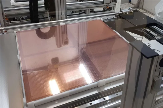
Lam Research’s inauguration of the Panel-Level Packaging (PLP) Innovation Excellence Center in Salzburg, Austria, represents a strategic pivot toward solving the ’economic wall’ of semiconductor manufacturing. As the industry moves toward heterogeneous integration—combining multiple specialized dies into a single package—the costs associated with traditional wafer-level packaging (WLP) on 300mm substrates are skyrocketing. PLP offers a radical departure by utilizing large rectangular panels (often 600mm x 600mm or larger), which provide approximately four times the usable surface area of a standard wafer.
This shift promises a significant reduction in cost-per-area, yet it introduces formidable mechanical and chemical engineering challenges that Lam Research is now addressing at the molecular level.
At the heart of Lam Research’s PLP strategy is its industry-leading Dielectric Atomic Layer Deposition (ALD) technology. Aaron Fellis, Corporate VP and General Manager of Dielectric ALD products, identifies the deposition of uniform insulating layers as the most critical hurdle for panel-scale adoption. Unlike traditional chemical vapor deposition (CVD), ALD allows for the sequential, self-limiting deposition of materials like Al2O3 or SiO2, ensuring perfect step coverage and film density across the vast topography of a 600mm panel.
This precision is vital for the creation of Redistribution Layers (RDL) that connect the chiplets. Without the uniformity provided by ALD, the electrical impedance between chips on the edge of the panel versus those in the center would vary wildly, leading to systemic yield failure. Furthermore, ALD films can be engineered to manage the coefficient of thermal expansion (CTE) mismatches that lead to panel warpage—a phenomenon where the large substrate bends during thermal cycling, making subsequent lithography steps impossible.
The Salzburg center serves as a collaborative hub where top-tier IDMs (Integrated Device Manufacturers) and OSATs can validate PLP process flows in a simulated high-volume manufacturing (HVM) environment. While PLP has been ‘just around the corner’ for several years, the lack of standardized equipment and material sets has stalled widespread adoption. Lam Research’s move to centralize PLP R&D in Austria signals a push to establish these missing standards.
By focusing on process control and metrology for large-format substrates, Lam is positioning its equipment as the foundational infrastructure for the next generation of AI and mobile hardware. The success of this center could effectively shift the center of gravity for advanced packaging innovation from Asia toward a more globally distributed model, leveraging European expertise in precision engineering and material science to meet the demands of the AI era.


