🔍 Executive Summary
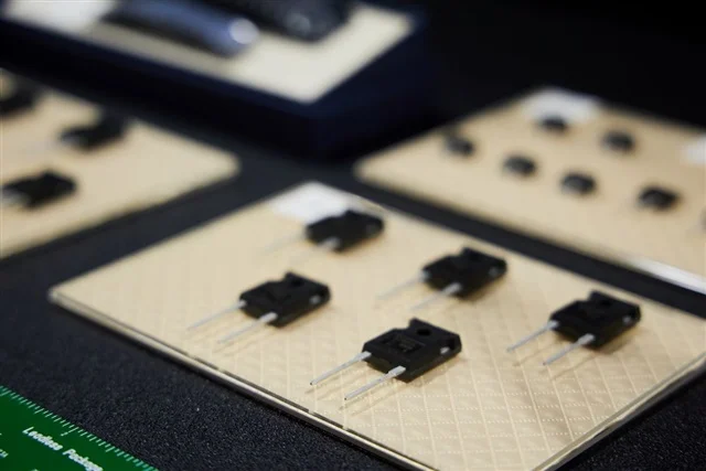
- Huawei’s unveiling of a 122TB enterprise-grade SSD marks a pivotal moment in the ongoing semiconductor trade war, highlighting a strategic shift from node-level scaling to advanced packaging innovation. Faced with stringent US sanctions that prohibit the acquisition of 232-layer and higher 3D NAND chips—technologies heavily dependent on American EDA tools and deposition equipment—Huawei has turned to a proprietary 'Die-on-Board' (COB) architecture. This engineering workaround bypasses traditional NAND packaging standards, such as Ball Grid Array (BGA), by mounting raw NAND dies directly onto t...
Strategic Deep-Dive
Huawei’s unveiling of a 122TB enterprise-grade SSD marks a pivotal moment in the ongoing semiconductor trade war, highlighting a strategic shift from node-level scaling to advanced packaging innovation. Faced with stringent US sanctions that prohibit the acquisition of 232-layer and higher 3D NAND chips—technologies heavily dependent on American EDA tools and deposition equipment—Huawei has turned to a proprietary ‘Die-on-Board’ (COB) architecture. This engineering workaround bypasses traditional NAND packaging standards, such as Ball Grid Array (BGA), by mounting raw NAND dies directly onto the printed circuit board (PCB).
By eliminating the physical overhead of individual chip packages, Huawei can populate the PCB with a significantly higher quantity of lower-density, non-sanctioned NAND dies.
From a senior analyst’s perspective, this approach is a masterclass in ‘system-level scaling.’ While Western rivals like Solidigm or Micron achieve high capacities through vertical density (increasing layers per die), Huawei is achieving it through spatial optimization. However, the engineering trade-offs are non-trivial. First, thermal management becomes a critical bottleneck.
In a traditional SSD, the package acts as a buffer and a primary heat spreader. In a die-on-board configuration, the heat generated by hundreds of active NAND dies is concentrated directly on the substrate, requiring sophisticated thermal interface materials (TIM) and custom-engineered airflow solutions within the server chassis to prevent thermal throttling. Second, the impact on manufacturing yields is a concern.
In modular designs, a faulty NAND package can be replaced; in a massive COB layout, a single die failure post-soldering could potentially jeopardize the entire 122TB module, significantly increasing the Total Cost of Ownership (TCO) if reliability standards are not met.
Despite these challenges, the implications for the global storage market are profound. Huawei is demonstrating that even without access to the latest sub-10nm equivalent NAND nodes, it can remain competitive in the high-density storage market required for AI training and big data analytics. This development signals that the ‘packaging wall’ is the new frontier for Chinese firms.
By leveraging domestic outsourced semiconductor assembly and test (OSAT) capabilities to refine die-on-board techniques, Huawei is effectively decoupling its product roadmap from the cadence of Western equipment manufacturers. For enterprise data centers, this translates to a viable alternative that prioritizes sheer capacity and footprint efficiency over the power-performance benefits of high-layer 3D NAND. Ultimately, this 122TB SSD serves as a testament to the resilience of the Chinese hardware ecosystem, proving that architectural ingenuity can compensate for restricted access to cutting-edge silicon nodes, provided the firm can master the complexities of high-density board-level integration.