🔍 Executive Summary
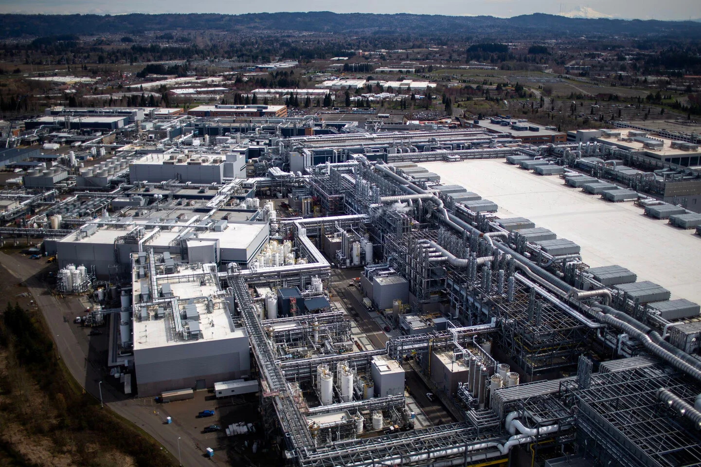
- The VLSI 2025 conference highlighted several foundational shifts in semiconductor physics and manufacturing logistics. Intel's 18A process took center stage, with detailed teardowns of its cost-per-wafer metrics and its reliance on RibbonFET architectures. A critical topic was the inevitable transition from 4F2 DRAM structures to 3D DRAM. As traditional 1T1C (one transistor, one capacitor) scaling hits a physical wall, 3D stacking of DRAM cells is becoming the only path forward for density improvements. In the logic sector, the adoption of Backside Power Delivery Networks (BSPDN) was analyzed ...
Strategic Deep-Dive
The VLSI 2025 conference highlighted several foundational shifts in semiconductor physics and manufacturing logistics. Intel’s 18A process took center stage, with detailed teardowns of its cost-per-wafer metrics and its reliance on RibbonFET architectures. A critical topic was the inevitable transition from 4F2 DRAM structures to 3D DRAM.
As traditional 1T1C (one transistor, one capacitor) scaling hits a physical wall, 3D stacking of DRAM cells is becoming the only path forward for density improvements. In the logic sector, the adoption of Backside Power Delivery Networks (BSPDN) was analyzed as a solution to parasitic resistance and routing congestion, though challenges in thermal dissipation and wafer-to-wafer bonding remain. Furthermore, the ‘Atoms to Fabs’ initiative underscored the rise of Digital Twins.
By using atomistic modeling to predict material behaviors at the nanometer scale and linking them to real-time fab logistics, manufacturers can optimize yields and reduce R&D cycles significantly. China’s showcase of the ‘FlipFET’ architecture also drew attention, representing a localized attempt to innovate in the Gate-All-Around (GAA) era. Collectively, these trends illustrate that semiconductor leadership now requires a holistic mastery of material science, 3D structural engineering, and comprehensive digital simulation of the entire fabrication environment.