핵심 요약
- ENG_TITLE: TSMC unveils A13 node as direct successor to A14 for next-generation AI compute…
상세 분석
ENG_TITLE: TSMC unveils A13 node as direct successor to A14 for next-generation AI compute
KOR_TITLE: TSMC, AI 연산 혁신을 위한 차세대 A13 공정 공개 및 옹스트롬 시대 선도
KEYWORDS_EN: TSMC, A13, Node Shrink, AI Hardware, Semiconductor Fabrication, A14, Angstrom Era
KEYWORDS_KR: TSMC, A13 공정, 미세 공정, AI 하드웨어, 반도체 파운드리, 옹스트롬, 공정 미세화
ENG_CONTENT
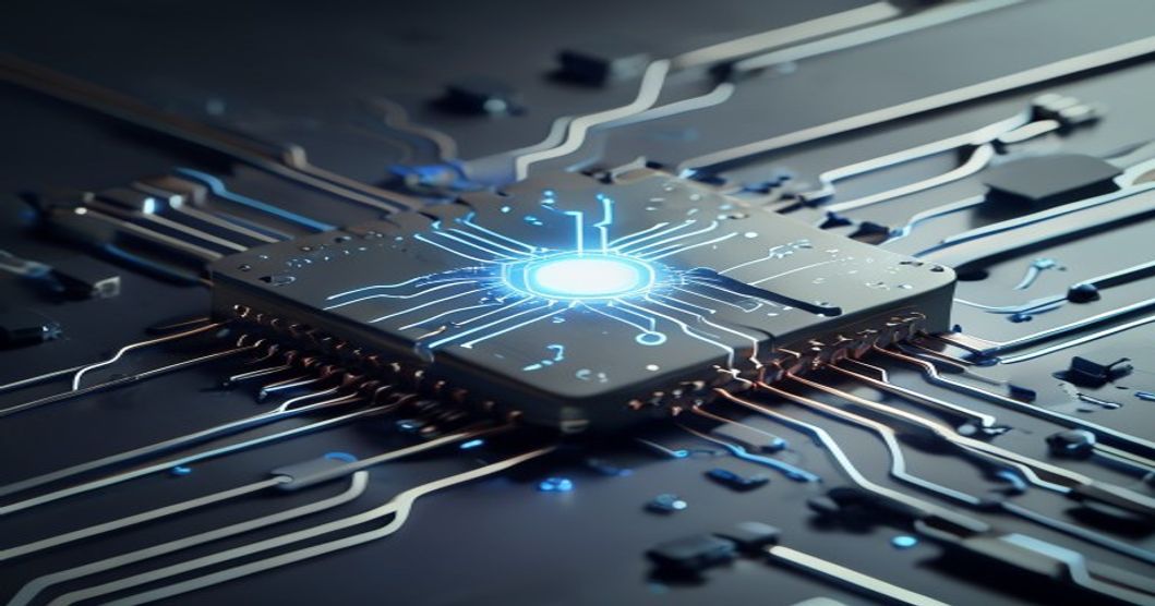
At the 2026 North America Technology Symposium, TSMC officially debuted the A13 process node, a critical addition to its “Angstrom-class” roadmap. Positioned as a direct successor to the A14 node announced last year, the A13 is characterized as a “direct shrink.” In the complex world of semiconductor lithography, a direct shrink is a highly strategic move that optimizes the existing gate-all-around (GAA) transistor architecture to achieve higher density and improved power-performance metrics without the long lead times associated with a completely new platform architecture. This allows lead customers, particularly in the AI accelerator and mobile SoC sectors, to achieve a faster Time-to-Market (TTM) for their next-generation products.
The naming convention itself marks a new phase in the “node war” between TSMC, Intel, and Samsung. With Intel aggressively marketing its 14A node, TSMC’s A13 is a clear tactical response designed to maintain its lead in logic density and power efficiency. While the A14 focused on the initial implementation of advanced backside power delivery, the A13 refines these features to squeeze out additional performance-per-watt gains.
This is crucial because, in 2026, the industry is no longer just fighting for the smallest transistor, but for the best thermal management at the wafer level. As AI chips push 1,000 watts and beyond, any efficiency gain from the fabrication node directly translates into lower cooling costs for the end data center operator.
From a market perspective, the A13 node arrives at a time of “insatiable customer demand.” Hyperscalers are currently engaged in a massive hardware upgrade cycle, moving from 5nm and 3nm designs to 2nm-class (A-series) hardware. The A13 offers a sweet spot in the manufacturing curve; it leverages the yield-learning from the A14 while providing the “compact design” benefits necessary for Edge AI devices where battery life and form factor are paramount. By offering A13 as a refined, high-yield alternative to the earlier A14, TSMC ensures that its N2/N3 capacity transitions smoothly into the A-series era without the production bottlenecks that sometimes plague first-generation nodes.
Technically, the A13 node is expected to feature advanced packaging compatibility, specifically targeting CoWoS (Chip-on-Wafer-on-Substrate) and SoIC (System-on-Integrated-Chips) technologies. This integration is vital for the upcoming 2027 generation of AI accelerators that will require tighter integration between logic and HBM4. TSMC’s mastery of both the frontend fabrication (A13) and the backend advanced packaging allows it to offer a turnkey solution that rivals find difficult to match.
As we look at the competitive landscape, the A13 reinforces TSMC’s status as the “foundry of choice” for the world’s most sophisticated AI workloads.
KOR_CONTENT
차세대 A13 공정의 기술적 정의와 옹스트롬 시대의 도래
TSMC가 2026 북미 기술 심포지엄에서 차세대 미세 공정인 A13을 전격 공개했습니다. A13은 지난해 발표된 A14 노드의 ‘다이렉트 슈링크(Direct Shrink)’ 버전으로, 기존의 옹스트롬(Angstrom)급 아키텍처를 고도화하여 소자 밀도와 전력 효율을 극대화한 것이 특징입니다. 이는 단순히 회로 선폭을 줄이는 것을 넘어, GAA(Gate-All-Around) 트랜지스터 구조의 안정성을 확보하고 고객사들에게 더 빠른 시장 출시(Time-to-Market) 기회를 제공하기 위한 TSMC의 전략적 선택으로 풀이됩니다.
인텔 14A와의 경쟁 및 공정 미세화의 가치
반도체 업계의 노드 명칭 경쟁이 치열해지는 가운데, TSMC의 A13은 인텔의 14A 공정에 대응하는 강력한 무기가 될 전망입니다. A13은 특히 후면 전력 공급(Backside Power Delivery) 기술을 정교화하여 와트당 성능을 획기적으로 개선했습니다. 2026년 현재 AI 반도체들이 직면한 최대 과제인 발열 문제를 공정 수준에서 해결함으로써, 데이터 센터 운영 비용을 절감하고자 하는 글로벌 하이퍼스케일러들의 요구를 완벽히 충족시킬 것으로 보입니다.
AI 및 에지 컴퓨팅을 위한 최적화 솔루션
A13 공정은 폭발적인 AI 연산 수요와 모바일 기기의 에지 AI 성능 향상을 동시에 겨냥하고 있습니다. TSMC는 A14에서 축적한 수율(Yield) 노하우를 A13에 적용하여 생산 안정성을 높이는 동시에, CoWoS 및 SoIC와 같은 첨단 패키징 기술과의 결합을 최적화했습니다. 이를 통해 차세대 AI 가속기와 고성능 워크스테이션용 칩셋 제조사들은 더욱 작고 강력한 하드웨어를 설계할 수 있게 되었습니다.
TSMC는 A13을 통해 파운드리 시장에서의 압도적인 기술 우위를 다시 한번 입증하며 시장 점유율 1위 자리를 확고히 할 것으로 기대됩니다.
IMAGE_PROMPT: A macro shot of a sophisticated 2nm-class silicon wafer with intricate circuitry glowing in electric blue, featuring the TSMC logo in a high-tech cleanroom environment.
ORIGINAL_URL: https://www.techpowerup.com/img/GPZCLcxCd1f8wcke.jpg